- 您現(xiàn)在的位置:買賣IC網(wǎng) > PDF目錄1978 > AD5348BCPZ (Analog Devices Inc)IC DAC 12BIT OCTAL VOUT 40LFCSP PDF資料下載
參數(shù)資料
| 型號: | AD5348BCPZ |
| 廠商: | Analog Devices Inc |
| 文件頁數(shù): | 1/24頁 |
| 文件大小: | 0K |
| 描述: | IC DAC 12BIT OCTAL VOUT 40LFCSP |
| 產(chǎn)品培訓(xùn)模塊: | Data Converter Fundamentals DAC Architectures |
| 標(biāo)準(zhǔn)包裝: | 1 |
| 設(shè)置時間: | 8µs |
| 位數(shù): | 12 |
| 數(shù)據(jù)接口: | 并聯(lián) |
| 轉(zhuǎn)換器數(shù)目: | 8 |
| 電壓電源: | 單電源 |
| 功率耗散(最大): | 8.3mW |
| 工作溫度: | -40°C ~ 105°C |
| 安裝類型: | 表面貼裝 |
| 封裝/外殼: | 40-VFQFN 裸露焊盤,CSP |
| 供應(yīng)商設(shè)備封裝: | 40-LFCSP |
| 包裝: | 托盤 |
| 輸出數(shù)目和類型: | 8 電壓,單極;8 電壓,雙極 |
| 采樣率(每秒): | 125k |
2.5 V to 5.5 V, Parallel Interface
Octal Voltage Output 8-/10-/12-Bit DACs
AD5346/AD5347/AD5348
Rev. 0
Information furnished by Analog Devices is believed to be accurate and reliable.
However, no responsibility is assumed by Analog Devices for its use, nor for any
infringements of patents or other rights of third parties that may result from its use.
Specifications subject to change without notice. No license is granted by implication
or otherwise under any patent or patent rights of Analog Devices. Trademarks and
registered trademarks are the property of their respective owners.
One Technology Way, P.O. Box 9106, Norwood, MA 02062-9106, U.S.A.
Tel: 781.329.4700
Fax: 781.326.8703
2003 Analog Devices, Inc. All rights reserved.
FEATURES
AD5346: octal 8-bit DAC
AD5347: octal 10-bit DAC
AD5348: octal 12-bit DAC
Low power operation: 1.4 mA (max) @ 3.6 V
Power-down to 120 nA @ 3 V, 400 nA @ 5 V
Guaranteed monotonic by design over all codes
Rail-to-rail output range: 0 V to VREF or 0 V to 2 × VREF
Power-on reset to 0 V
Simultaneous update of DAC outputs via LDAC pin
Asynchronous CLR facility
Readback
Buffered/unbuffered reference inputs
20 ns WR time
38-lead TSSOP/6 mm × 6 mm 40-lead LFCSP packaging
Temperature range: –40°C to +105°C
APPLICATIONS
Portable battery-powered instruments
Digital gain and offset adjustment
Programmable voltage and current sources
Optical networking
Automatic test equipment
Mobile communications
Programmable attenuators
Industrial process control
GENERAL DESCRIPTION
The AD5346/AD5347/AD53481 are octal 8-, 10-, and 12-bit
DACs, operating from a 2.5 V to 5.5 V supply. These devices
incorporate an on-chip output buffer that can drive the output
to both supply rails, and also allow a choice of buffered or
unbuffered reference input.
The AD5346/AD5347/AD5348 have a parallel interface. CS
selects the device and data is loaded into the input registers on
the rising edge of WR. A readback feature allows the internal
DAC registers to be read back through the digital port.
The GAIN pin on these devices allows the output range to be
set at 0 V to VREF or 0 V to 2 × VREF.
Input data to the DACs is double-buffered, allowing simultane-
ous update of multiple DACs in a system using the LDAC pin.
An asynchronous CLR input is also provided, which resets the
contents of the input register and the DAC register to all zeros.
These devices also incorporate a power-on reset circuit that
ensures that the DAC output powers on to 0 V and remains
there until valid data is written to the device.
All three parts are pin compatible, which allows users to select
the amount of resolution appropriate for their application
without redesigning their circuit board.
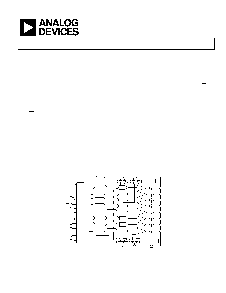
FUNCTIONAL BLOCK DIAGRAM
INPUT
REGISTER
DAC
REGISTER
STRING
DAC C
STRING
DAC A
STRING
DAC B
STRING
DAC D
STRING
DAC E
STRING
DAC F
STRING
DAC G
STRING
DAC H
DGND
VOUTB
VOUTC
VOUTD
VOUTE
VOUTG
VOUTH
VOUTF
VDD
POWER-ON
RESET
VOUTA
VREFEF
VREFAB
PD
INTER-
FACE
LOGIC
GAIN
DB11
DB0
CS
WR
A0
A1
CLR
LDAC
.
BUF
A2
RD
VREFGH
VREFCD
AGND
BUFFER
INPUT
REGISTER
INPUT
REGISTER
INPUT
REGISTER
INPUT
REGISTER
INPUT
REGISTER
INPUT
REGISTER
INPUT
REGISTER
DAC
REGISTER
DAC
REGISTER
DAC
REGISTER
DAC
REGISTER
DAC
REGISTER
DAC
REGISTER
DAC
REGISTER
AD5348
POWER-DOWN
LOGIC
03331-
0-
001
Figure 1.
1Protected by U.S. Patent No. 5,969,657.
相關(guān)PDF資料 |
PDF描述 |
|---|---|
| AD5361BSTZ | IC DAC 14BIT 16CH SERIAL 56LQFP |
| AD5363BSTZ | IC DAC 14BIT 8CH SERIAL 52-LQFP |
| AD5370BSTZ | IC DAC 16BIT 40CH SERIAL 64-LQFP |
| AD5373BSTZ | IC DAC 14BIT 32CH SER 64-LQFP |
| AD5378ABC | IC DAC 14BIT 32CHAN 108CSPBGA |
相關(guān)代理商/技術(shù)參數(shù) |
參數(shù)描述 |
|---|---|
| AD5348BCPZCPZ | 制造商:Analog Devices 功能描述:DAC,AD5348B 12bit 8us octal LFCSP |
| AD5348BRU | 功能描述:IC DAC 12BIT OCTAL VOUT 38-TSSOP RoHS:否 類別:集成電路 (IC) >> 數(shù)據(jù)采集 - 數(shù)模轉(zhuǎn)換器 系列:- 產(chǎn)品培訓(xùn)模塊:Data Converter Fundamentals DAC Architectures 標(biāo)準(zhǔn)包裝:750 系列:- 設(shè)置時間:7µs 位數(shù):16 數(shù)據(jù)接口:并聯(lián) 轉(zhuǎn)換器數(shù)目:1 電壓電源:雙 ± 功率耗散(最大):100mW 工作溫度:0°C ~ 70°C 安裝類型:表面貼裝 封裝/外殼:28-LCC(J 形引線) 供應(yīng)商設(shè)備封裝:28-PLCC(11.51x11.51) 包裝:帶卷 (TR) 輸出數(shù)目和類型:1 電壓,單極;1 電壓,雙極 采樣率(每秒):143k |
| AD5348BRU-REEL | 功能描述:IC DAC 12BIT OCTAL VOUT 38-TSSOP RoHS:否 類別:集成電路 (IC) >> 數(shù)據(jù)采集 - 數(shù)模轉(zhuǎn)換器 系列:- 產(chǎn)品培訓(xùn)模塊:Data Converter Fundamentals DAC Architectures 標(biāo)準(zhǔn)包裝:750 系列:- 設(shè)置時間:7µs 位數(shù):16 數(shù)據(jù)接口:并聯(lián) 轉(zhuǎn)換器數(shù)目:1 電壓電源:雙 ± 功率耗散(最大):100mW 工作溫度:0°C ~ 70°C 安裝類型:表面貼裝 封裝/外殼:28-LCC(J 形引線) 供應(yīng)商設(shè)備封裝:28-PLCC(11.51x11.51) 包裝:帶卷 (TR) 輸出數(shù)目和類型:1 電壓,單極;1 電壓,雙極 采樣率(每秒):143k |
| AD5348BRU-REEL7 | 功能描述:IC DAC 12BIT OCTAL VOUT 38-TSSOP RoHS:否 類別:集成電路 (IC) >> 數(shù)據(jù)采集 - 數(shù)模轉(zhuǎn)換器 系列:- 產(chǎn)品培訓(xùn)模塊:Data Converter Fundamentals DAC Architectures 標(biāo)準(zhǔn)包裝:750 系列:- 設(shè)置時間:7µs 位數(shù):16 數(shù)據(jù)接口:并聯(lián) 轉(zhuǎn)換器數(shù)目:1 電壓電源:雙 ± 功率耗散(最大):100mW 工作溫度:0°C ~ 70°C 安裝類型:表面貼裝 封裝/外殼:28-LCC(J 形引線) 供應(yīng)商設(shè)備封裝:28-PLCC(11.51x11.51) 包裝:帶卷 (TR) 輸出數(shù)目和類型:1 電壓,單極;1 電壓,雙極 采樣率(每秒):143k |
| AD5348BRUZ | 功能描述:IC DAC 12BIT OCTAL VOUT 38-TSSOP RoHS:是 類別:集成電路 (IC) >> 數(shù)據(jù)采集 - 數(shù)模轉(zhuǎn)換器 系列:- 產(chǎn)品培訓(xùn)模塊:Lead (SnPb) Finish for COTS Obsolescence Mitigation Program 標(biāo)準(zhǔn)包裝:50 系列:- 設(shè)置時間:4µs 位數(shù):12 數(shù)據(jù)接口:串行 轉(zhuǎn)換器數(shù)目:2 電壓電源:單電源 功率耗散(最大):- 工作溫度:-40°C ~ 85°C 安裝類型:表面貼裝 封裝/外殼:8-TSSOP,8-MSOP(0.118",3.00mm 寬) 供應(yīng)商設(shè)備封裝:8-uMAX 包裝:管件 輸出數(shù)目和類型:2 電壓,單極 采樣率(每秒):* 產(chǎn)品目錄頁面:1398 (CN2011-ZH PDF) |
發(fā)布緊急采購,3分鐘左右您將得到回復(fù)。