- 您現(xiàn)在的位置:買賣IC網(wǎng) > PDF目錄8579 > AD5544BRSZ-REEL7 (Analog Devices Inc)IC DAC 16BIT QUAD SRL 28SSOP PDF資料下載
參數(shù)資料
| 型號: | AD5544BRSZ-REEL7 |
| 廠商: | Analog Devices Inc |
| 文件頁數(shù): | 1/24頁 |
| 文件大小: | 0K |
| 描述: | IC DAC 16BIT QUAD SRL 28SSOP |
| 標(biāo)準(zhǔn)包裝: | 500 |
| 設(shè)置時間: | 900ns |
| 位數(shù): | 16 |
| 數(shù)據(jù)接口: | 串行,SPI? |
| 轉(zhuǎn)換器數(shù)目: | 4 |
| 電壓電源: | 雙 ± |
| 功率耗散(最大): | 1.25mW |
| 工作溫度: | -40°C ~ 125°C |
| 安裝類型: | 表面貼裝 |
| 封裝/外殼: | 28-SSOP(0.209",5.30mm 寬) |
| 供應(yīng)商設(shè)備封裝: | 28-SSOP |
| 包裝: | 帶卷 (TR) |
| 輸出數(shù)目和類型: | 4 電流,單極;4 電流,雙極 |
Quad, Current-Output,
Serial-Input 16-/14-Bit DACs
Data Sheet
Rev. G
Information furnished by Analog Devices is believed to be accurate and reliable. However, no
responsibilityisassumedbyAnalogDevicesforitsuse,norforanyinfringementsofpatentsorother
rightsofthirdpartiesthatmayresultfromitsuse.Specificationssubjecttochangewithoutnotice.No
license is granted by implication or otherwise under any patent or patent rights of Analog Devices.
Trademarksandregisteredtrademarksarethepropertyoftheirrespectiveowners.
One Technology Way, P.O. Box 9106, Norwood, MA 02062-9106, U.S.A.
Tel: 781.329.4700
2000–2013 Analog Devices, Inc. All rights reserved.
FEATURES
AD5544: 16-bit resolution
INL of ±1 LSB (B Grade)
AD5554: 14-bit resolution
INL of ±0.5 LSB (B Grade)
2 mA full-scale current ± 20%, with VREF = ±10 V
0.9 s settling time to ±0.1%
12 MHz multiplying bandwidth
Midscale glitch of 1 nV-sec
Midscale or zero-scale reset
4 separate, 4-quadrant multiplying reference inputs
SPI-compatible, 3-wire interface
Double-buffered registers enable
Simultaneous multichannel change
Internal power-on reset
Temperature range: 40°C to +125°C
Compact 28-lead SSOP and 32-lead LFCSP
APPLICATIONS
Automatic test equipment
Instrumentation
Digitally controlled calibration
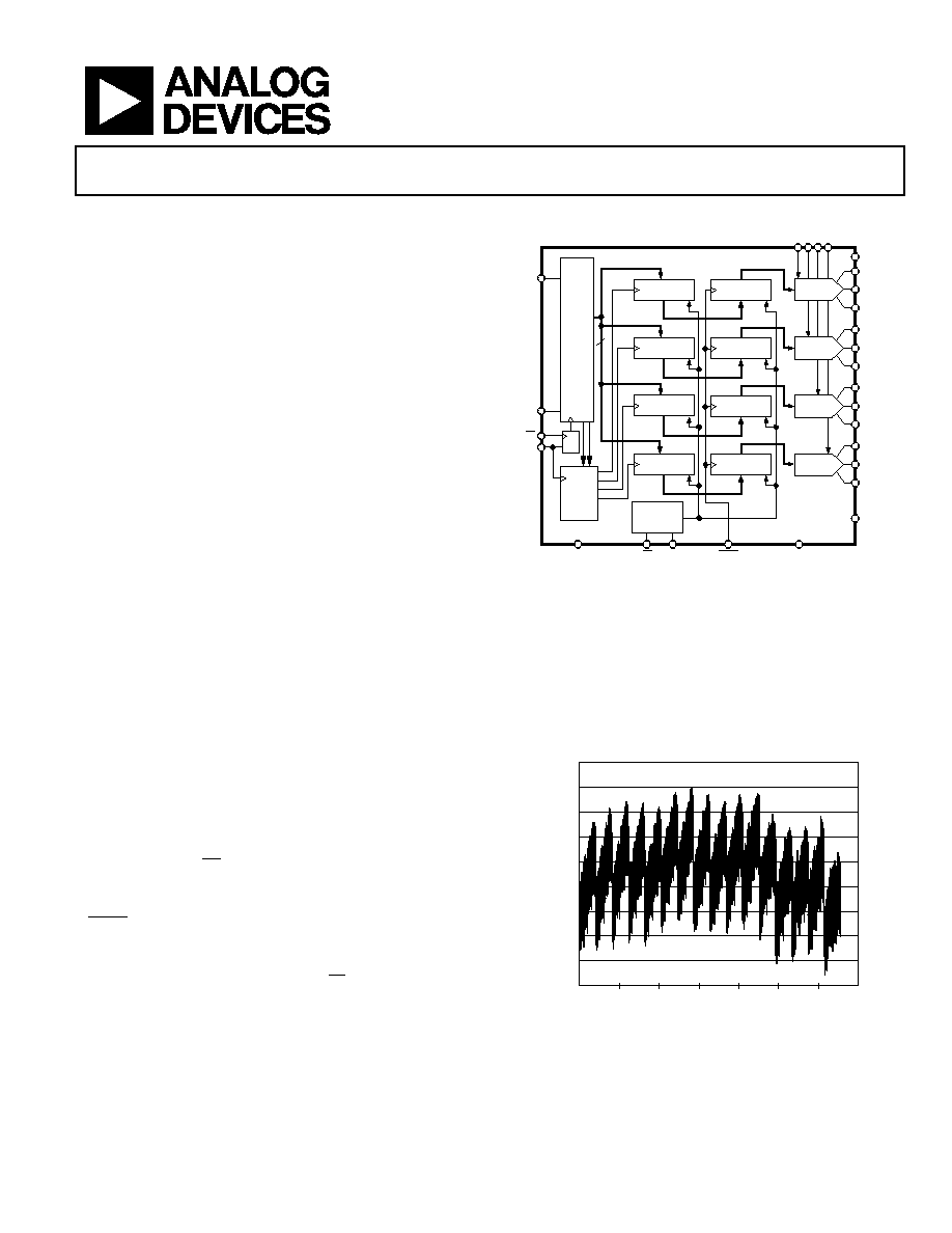
FUNCTIONAL BLOCK DIAGRAM
INPUT
REGISTER R
16
DAC A
REGISTER R
2:4
DECODE
DAC A
B
C
D
POWER-ON
RESET
D0
D1
D2
D3
D4
D5
D6
D7
D8
D9
D10
D11
D12
D13
D14
D15
A0
A1
EN
VDD
RFBA
IOUTA
AGNDA
AGNDF
VSS
LDAC
MSB
RS
DGND
CLK
CS
SDI
SDO
VREFA B C
RFBB
IOUTB
AGNDB
RFBC
IOUTC
AGNDC
RFBD
IOUTD
AGNDD
AD5544
INPUT
REGISTER R
INPUT
REGISTER R
INPUT
REGISTER R
DAC B
REGISTER R
DAC C
REGISTER R
DAC D
REGISTER R
D
DAC A
DAC B
DAC D
DAC C
00943-
001
Figure 1.
GENERAL DESCRIPTION
The AD5544/AD5554 quad, 16-/14-bit, current output, digital-
to-analog converters (DACs) are designed to operate from a
2.7 V to 5.5 V supply range.
The applied external reference input voltage (VREFx) determines
the full-scale output current. Integrated feedback resistors (RFB)
provide temperature-tracking, full-scale voltage outputs when
combined with an external I-to-V precision amplifier.
A double-buffered serial data interface offers high speed, 3-wire,
SPI- and microcontroller-compatible inputs using serial data in
(SDI), a chip select (CS), and clock (CLK) signals. In addition,
a serial data out pin (SDO) allows for daisy-chaining when multiple
packages are used. A common, level-sensitive, load DAC strobe
(LDAC) input allows the simultaneous update of all DAC outputs
from previously loaded input registers. Additionally, an internal
power-on reset forces the output voltage to 0 at system turn-on.
The MSB pin allows system reset assertion (RS) to force all registers
to zero code when MSB = 0 or to half-scale code when MSB = 1.
The AD5544 is packaged in the compact 28-lead SSOP and 32-
lead LFCSP. The AD5554 is packed in the compact 28-lead SSOP.
The EV-AD5544/45SDZ is available for evaluating DAC perfor-
mance. For more information, see the UG-285 evaluation board
user guide.
0.7
0.6
0.5
0.4
0.3
0.2
0.1
0
–0.1
–0.2
0
10,000
30,000
50,000
70,000
00943-
002
INL
E
RRO
R
(
L
S
B)
CODE
20,000
40,000
60,000
相關(guān)PDF資料 |
PDF描述 |
|---|---|
| VE-26H-MY-B1 | CONVERTER MOD DC/DC 52V 50W |
| NCS2563DR2G | IC VIDEO AMP 3CH HD FILTER 8SOIC |
| VE-26F-MY-B1 | CONVERTER MOD DC/DC 72V 50W |
| VE-25F-MY-B1 | CONVERTER MOD DC/DC 72V 50W |
| ADDAC80N-CBI-V | IC DAC 12-BIT BINARY MONO 24-DIP |
相關(guān)代理商/技術(shù)參數(shù) |
參數(shù)描述 |
|---|---|
| AD5544EVAL | 制造商:AD 制造商全稱:Analog Devices 功能描述:Quad, Current-Output, Serial-Input 16-/14-Bit DACs |
| AD5544SRS-EP | 功能描述:數(shù)模轉(zhuǎn)換器- DAC QUAD 16-BIT DAC RoHS:否 制造商:Texas Instruments 轉(zhuǎn)換器數(shù)量:1 DAC 輸出端數(shù)量:1 轉(zhuǎn)換速率:2 MSPs 分辨率:16 bit 接口類型:QSPI, SPI, Serial (3-Wire, Microwire) 穩(wěn)定時間:1 us 最大工作溫度:+ 85 C 安裝風(fēng)格:SMD/SMT 封裝 / 箱體:SOIC-14 封裝:Tube |
| AD5545 | 制造商:AD 制造商全稱:Analog Devices 功能描述:Dual, Current-Output, Serial-Input, 16-/14-Bit DAC |
| AD5545BRU | 功能描述:IC DAC 16BIT DUAL SRL IN 16TSSOP RoHS:否 類別:集成電路 (IC) >> 數(shù)據(jù)采集 - 數(shù)模轉(zhuǎn)換器 系列:- 標(biāo)準(zhǔn)包裝:2,400 系列:- 設(shè)置時間:- 位數(shù):18 數(shù)據(jù)接口:串行 轉(zhuǎn)換器數(shù)目:3 電壓電源:模擬和數(shù)字 功率耗散(最大):- 工作溫度:-40°C ~ 85°C 安裝類型:表面貼裝 封裝/外殼:36-TFBGA 供應(yīng)商設(shè)備封裝:36-TFBGA 包裝:帶卷 (TR) 輸出數(shù)目和類型:* 采樣率(每秒):* |
| AD5545BRU-REEL7 | 制造商:Analog Devices 功能描述:DAC 2-CH R-2R/Current Steering 16-bit 16-Pin TSSOP T/R |
發(fā)布緊急采購,3分鐘左右您將得到回復(fù)。