- 您現在的位置:買賣IC網 > PDF目錄22156 > AD652KP (Analog Devices Inc)IV V-F CONVERTER SYNC 20-PLCC PDF資料下載
參數資料
| 型號: | AD652KP |
| 廠商: | Analog Devices Inc |
| 文件頁數: | 1/28頁 |
| 文件大小: | 779K |
| 描述: | IV V-F CONVERTER SYNC 20-PLCC |
| 標準包裝: | 1 |
| 類型: | 電壓至頻率 |
| 頻率 - 最大: | 2MHz |
| 全量程: | ±25ppm/°C |
| 線性: | ±0.005% |
| 安裝類型: | 表面貼裝 |
| 封裝/外殼: | 20-LCC(J 形引線) |
| 供應商設備封裝: | 20-PLCC(9x9) |
| 包裝: | 管件 |
當前第1頁第2頁第3頁第4頁第5頁第6頁第7頁第8頁第9頁第10頁第11頁第12頁第13頁第14頁第15頁第16頁第17頁第18頁第19頁第20頁第21頁第22頁第23頁第24頁第25頁第26頁第27頁第28頁
Monolithic Synchronous
Voltage-to-Frequency Converter
AD652
Rev. C
Information furnished by Analog Devices is believed to be accurate and reliable.
However, no responsibility is assumed by Analog Devices for its use, nor for any
infringements of patents or other rights of third parties that may result from its use.
Specifications subject to change without notice. No license is granted by implication
or otherwise under any patent or patent rights of Analog Devices. Trademarks and
registered trademarks are the property of their respective owners.
One Technology Way, P.O. Box 9106, Norwood, MA 02062-9106, U.S.A.
Tel: 781.329.4700
www.analog.com
Fax: 781.326.8703 ?2004 Analog Devices, Inc. All rights reserved.
FEATURES
Full-scale frequency (up to 2 MHz) set by external system
clock
Extremely low linearity error (0.005% max at 1 MHz FS,
0.02% max at 2 MHz FS)
No critical external components required
Accurate 5 V reference voltage
Low drift (25 ppm/?/SPAN>C max)
Dual- or single-supply operation
Voltage or current input
MIL-STD-883 compliant versions available
PRODUCT DESCRIPTION
The AD652 synchronous voltage-to-frequency converter
(SVFC) is a powerful building block for precision analog-to-
digital conversion, offering typical nonlinearity of 0.002%
(0.005% maximum) at a 100 kHz output frequency. The inher-
ent monotonicity of the transfer function and wide range of
clock frequencies allow the conversion time and resolution to
be optimized for specific applications.
The AD652 uses a variation of the charge-balancing technique
to perform the conversion function. The AD652 uses an
external clock to define the full-scale output frequency, rather
than relying on the stability of an external capacitor. The result
is a more stable, more linear transfer function, with significant
application benefits in both single- and multichannel systems.
Gain drift is minimized using a precision low drift reference
and low TC, on-chip, thin-film scaling resistors. Furthermore,
initial gain error is reduced to less than 0.5% by the use of laser-
wafer-trimming.
The analog and digital sections of the AD652 have been
designed to allow operation from a single-ended power source,
simplifying its use with isolated power supplies.
The AD652 is available in five performance grades. The 20-lead
PLCC-packaged JP and KP grades are specified for operation
over the 0癈 to +70癈 commercial temperature range. The
16-lead CERDIP-packaged AQ and BQ grades are specified for
operation over the 40癈 to +85癈 industrial temperature
range. The AD652SQ is available for operation over the full
55癈 to +125癈 extended temperature range.
PRODUCT HIGHLIGHTS
1. The use of an external clock to set the full-scale frequency
allows the AD652 to achieve linearity and stability far
superior to other monolithic VFCs. By using the same clock
to drive the AD652 and set the counting period (through a
suitable divider), conversion accuracy is maintained
independent of variations in clock frequency.
2. The AD652 synchronous VFC requires only one external
component (a noncritical integrator capacitor) for
operation.
3. The AD652 includes a buffered, accurate 5 V reference.
4. The AD652s clock input is TTL and CMOS compatible and
can also be driven by sources referred to the negative power
supply. The flexible open-collector output stage provides
sufficient current sinking capability for TTL and CMOS
logic, as well as for optical couplers and pulse transformers.
A capacitor-programmable one-shot is provided for selec-
tion of optimum output pulse width for power reduction.
5. The AD652 can also be configured for use as a synchronous
F/V converter for isolated analog signal transmission.
6. The AD652 is available in versions compliant with
MILSTD-883. Refer to the Analog Devices Military
Products Databook or current AD652/883B data sheet for
detailed specifications.
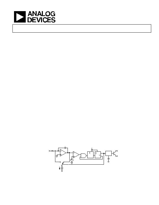
FUNCTIONAL BLOCK DIAGRAM
COMPARATOR
AND
CK
Q
D
G
Q
D
Q
D FLOP
LATCH
CLOCK IN
ONE
SHOT
C
OS
5V
C
INT
R
IN
INTEGRATOR
H L
1mA
V
S
V
IN
Figure 1.
相關PDF資料 |
PDF描述 |
|---|---|
| RCC65DRAI | CONN EDGECARD 130PS R/A .100 SLD |
| RBB108DHFN | CONN EDGECARD 216POS .050 SMD |
| RBB108DHFD | CONN EDGECARD 216POS .050 SMD |
| AD650KN | IC V-F/F-V CONVERTER 14-DIP |
| RBB45DHAR | CONN EDGECARD 90POS R/A .050 DIP |
相關代理商/技術參數 |
參數描述 |
|---|---|
| AD652KP-REEL | 制造商:Analog Devices 功能描述: |
| AD652KPZ | 功能描述:IV V-F CONVERTER SYNC 20-PLCC RoHS:是 類別:集成電路 (IC) >> PMIC - V/F 和 F/V 轉換器 系列:- 標準包裝:1 系列:- 類型:頻率至電壓 頻率 - 最大:10kHz 全量程:- 線性:±0.3% 安裝類型:表面貼裝 封裝/外殼:8-SOIC(0.154",3.90mm 寬) 供應商設備封裝:8-SOIC 包裝:Digi-Reel® 其它名稱:LM2917MX-8/NOPBDKR |
| AD652KPZ | 制造商:Analog Devices 功能描述:IC VOLTAGE CONVERTER |
| AD652KPZ-REEL | 功能描述:IC V-F CONVERTER SYNC 20PLCC RoHS:是 類別:集成電路 (IC) >> PMIC - V/F 和 F/V 轉換器 系列:- 標準包裝:1 系列:- 類型:頻率至電壓 頻率 - 最大:10kHz 全量程:- 線性:±0.3% 安裝類型:表面貼裝 封裝/外殼:8-SOIC(0.154",3.90mm 寬) 供應商設備封裝:8-SOIC 包裝:Digi-Reel® 其它名稱:LM2917MX-8/NOPBDKR |
| AD652SE/883B | 功能描述:電壓頻率轉換及頻率電壓轉換 IC - SYNC V/F CONVERTER RoHS:否 制造商:Texas Instruments 全標度頻率:4000 KHz 線性誤差:+/- 1 % FSR 電源電壓-最大: 電源電壓-最小: 最大工作溫度:+ 85 C 最小工作溫度:- 25 C 安裝風格:Through Hole 封裝 / 箱體:PDIP-14 封裝:Tube |
發布緊急采購,3分鐘左右您將得到回復。