參數資料
| 型號: | AD7528JPZ |
| 廠商: | Analog Devices Inc |
| 文件頁數: | 1/8頁 |
| 文件大小: | 0K |
| 描述: | IC DAC 8BIT DUAL MULT 20PLCC |
| 產品培訓模塊: | Data Converter Fundamentals DAC Architectures |
| 標準包裝: | 49 |
| 設置時間: | 400ns |
| 位數: | 8 |
| 數據接口: | 并聯 |
| 轉換器數目: | 2 |
| 電壓電源: | 單電源 |
| 功率耗散(最大): | 450mW |
| 工作溫度: | -40°C ~ 85°C |
| 安裝類型: | 表面貼裝 |
| 封裝/外殼: | 20-LCC(J 形引線) |
| 供應商設備封裝: | 20-PLCC(9x9) |
| 包裝: | 管件 |
| 輸出數目和類型: | 2 電流,單極;2 電流,雙極 |
REV. B
Information furnished by Analog Devices is believed to be accurate and
reliable. However, no responsibility is assumed by Analog Devices for its
use, nor for any infringements of patents or other rights of third parties
which may result from its use. No license is granted by implication or
otherwise under any patent or patent rights of Analog Devices.
a
CMOS Dual 8-Bit
Buffered Multiplying DAC
AD7528
FEATURES
On-Chip Latches for Both DACs
+5 V to +15 V Operation
DACs Matched to 1%
Four Quadrant Multiplication
TTL/CMOS Compatible
Latch Free (Protection Schottkys not Required)
APPLICATIONS
Digital Control of:
Gain/Attenuation
Filter Parameters
Stereo Audio Circuits
X-Y Graphics
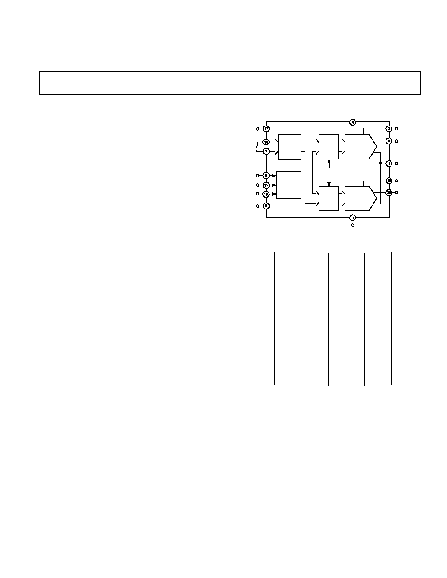
FUNCTIONAL BLOCK DIAGRAM
VREFA
AD7528
VREFB
RFB B
AGND
VDD
DB0
DB7
DATA
INPUTS
DAC A/
DAC B
CS
WR
DGND
CONTROL
LOGIC
INPUT
BUFFER
LATCH
OUT B
OUT A
DAC B
DAC A
RFB A
GENERAL DESCRIPTION
The AD7528 is a monolithic dual 8-bit digital/analog converter
featuring excellent DAC-to-DAC matching. It is available in
skinny 0.3" wide 20-lead DIPs and in 20-lead surface mount
packages.
Separate on-chip latches are provided for each DAC to allow
easy microprocessor interface.
Data is transferred into either of the two DAC data latches via a
common 8-bit TTL/CMOS compatible input port. Control
input
DAC A/DAC B determines which DAC is to be loaded.
The AD7528’s load cycle is similar to the write cycle of a ran-
dom access memory and the device is bus compatible with most
8-bit microprocessors, including 6800, 8080, 8085, Z80.
The device operates from a +5 V to +15 V power supply, dis-
sipating only 20 mW of power.
Both DACs offer excellent four quadrant multiplication charac-
teristics with a separate reference input and feedback resistor for
each DAC.
PRODUCT HIGHLIGHTS
1. DAC-to-DAC matching: since both of the AD7528 DACs are
fabricated at the same time on the same chip, precise match-
ing and tracking between DAC A and DAC B is inherent.
The AD7528’s matched CMOS DACs make a whole new
range of applications circuits possible, particularly in the
audio, graphics and process control areas.
2. Small package size: combining the inputs to the on-chip DAC
latches into a common data bus and adding a
DAC A/DAC B
select line has allowed the AD7528 to be packaged in either a
small 20-lead DIP, SOIC or PLCC.
ORDERING GUIDE
1
Temperature
Relative
Gain
Package
Model
2
Ranges
Accuracy Error
Options
3
AD7528JN
–40
°C to +85°C
±1 LSB
±4 LSB N-20
AD7528KN
–40
°C to +85°C
±1/2 LSB ±2 LSB N-20
AD7528LN
–40
°C to +85°C
±1/2 LSB ±1 LSB N-20
AD7528JP
–40
°C to +85°C
±1 LSB
±4 LSB P-20A
AD7528KP
–40
°C to +85°C
±1/2 LSB ±2 LSB P-20A
AD7528LP
–40
°C to +85°C
±1/2 LSB ±1 LSB P-20A
AD7528JR
–40
°C to +85°C
±1 LSB
±4 LSB R-20
AD7528KR
–40
°C to +85°C
±1/2 LSB ±2 LSB R-20
AD7528LR
–40
°C to +85°C
±1/2 LSB ±1 LSB R-20
AD7528AQ
–40
°C to +85°C
±1 LSB
±4 LSB Q-20
AD7528BQ
–40
°C to +85°C
±1/2 LSB ±2 LSB Q-20
AD7528CQ
–40
°C to +85°C
±1/2 LSB ±1 LSB Q-20
AD7528SQ
–55
°C to +125°C
±1 LSB
±4 LSB Q-20
AD7528TQ
–55
°C to +125°C
±1/2 LSB ±2 LSB Q-20
AD7528UQ
–55
°C to +125°C
±1/2 LSB ±1 LSB Q-20
NOTES
1Analog Devices reserves the right to ship side-brazed ceramic in lieu of cerdip. Parts
will be marked with cerdip designator “Q.”
2Processing to MIL-STD-883C, Class B is available. To order, add suffix “/883B” to
part number. For further information, see Analog Devices’ 1990 Military Products
Databook.
3N = Plastic DIP; P = Plastic Leaded Chip Carrier; Q = Cerdip; R = SOIC.
One Technology Way, P.O. Box 9106, Norwood, MA 02062-9106, U.S.A.
Tel: 781/329-4700
World Wide Web Site: http://www.analog.com
Fax: 781/326-8703
Analog Devices, Inc., 1998
相關PDF資料 |
PDF描述 |
|---|---|
| XR2206CP-F | IC FUNCTION GENERATOR 16PDIP |
| VE-21D-MW-F1 | CONVERTER MOD DC/DC 85V 100W |
| AD9752ARUZ | IC DAC 12BIT 125MSPS HP 28-TSSOP |
| M83723/85G22199 | CONN RCPT 19POS JAM NUT W/PINS |
| AD7224LRZ-18 | IC DAC 8BIT LC2MOS W/AMP 18SOIC |
相關代理商/技術參數 |
參數描述 |
|---|---|
| AD7528JPZ-REEL | 功能描述:IC DAC 8BIT DUAL MULT 20PLCC RoHS:是 類別:集成電路 (IC) >> 數據采集 - 數模轉換器 系列:- 標準包裝:47 系列:- 設置時間:2µs 位數:14 數據接口:并聯 轉換器數目:1 電壓電源:單電源 功率耗散(最大):55µW 工作溫度:-40°C ~ 85°C 安裝類型:表面貼裝 封裝/外殼:28-SSOP(0.209",5.30mm 寬) 供應商設備封裝:28-SSOP 包裝:管件 輸出數目和類型:1 電流,單極;1 電流,雙極 采樣率(每秒):* |
| AD7528JR | 功能描述:IC DAC 8BIT DUAL MULTIPLY 20SOIC RoHS:否 類別:集成電路 (IC) >> 數據采集 - 數模轉換器 系列:- 產品培訓模塊:Data Converter Fundamentals DAC Architectures 標準包裝:750 系列:- 設置時間:7µs 位數:16 數據接口:并聯 轉換器數目:1 電壓電源:雙 ± 功率耗散(最大):100mW 工作溫度:0°C ~ 70°C 安裝類型:表面貼裝 封裝/外殼:28-LCC(J 形引線) 供應商設備封裝:28-PLCC(11.51x11.51) 包裝:帶卷 (TR) 輸出數目和類型:1 電壓,單極;1 電壓,雙極 采樣率(每秒):143k |
| AD7528JR-REEL | 功能描述:IC DAC 8BIT DUAL MULT 20-SOIC RoHS:否 類別:集成電路 (IC) >> 數據采集 - 數模轉換器 系列:- 標準包裝:2,400 系列:- 設置時間:- 位數:18 數據接口:串行 轉換器數目:3 電壓電源:模擬和數字 功率耗散(最大):- 工作溫度:-40°C ~ 85°C 安裝類型:表面貼裝 封裝/外殼:36-TFBGA 供應商設備封裝:36-TFBGA 包裝:帶卷 (TR) 輸出數目和類型:* 采樣率(每秒):* |
| AD7528JR-REEL7 | 功能描述:IC DAC 8BIT DUAL MULT 20-SOIC RoHS:否 類別:集成電路 (IC) >> 數據采集 - 數模轉換器 系列:- 標準包裝:47 系列:- 設置時間:2µs 位數:14 數據接口:并聯 轉換器數目:1 電壓電源:單電源 功率耗散(最大):55µW 工作溫度:-40°C ~ 85°C 安裝類型:表面貼裝 封裝/外殼:28-SSOP(0.209",5.30mm 寬) 供應商設備封裝:28-SSOP 包裝:管件 輸出數目和類型:1 電流,單極;1 電流,雙極 采樣率(每秒):* |
| AD7528JRZ | 功能描述:IC DAC 8BIT DUAL MULT 20-SOIC RoHS:是 類別:集成電路 (IC) >> 數據采集 - 數模轉換器 系列:- 產品培訓模塊:Lead (SnPb) Finish for COTS Obsolescence Mitigation Program 標準包裝:50 系列:- 設置時間:4µs 位數:12 數據接口:串行 轉換器數目:2 電壓電源:單電源 功率耗散(最大):- 工作溫度:-40°C ~ 85°C 安裝類型:表面貼裝 封裝/外殼:8-TSSOP,8-MSOP(0.118",3.00mm 寬) 供應商設備封裝:8-uMAX 包裝:管件 輸出數目和類型:2 電壓,單極 采樣率(每秒):* 產品目錄頁面:1398 (CN2011-ZH PDF) |
發布緊急采購,3分鐘左右您將得到回復。