- 您現在的位置:買賣IC網 > PDF目錄373912 > AD7569KN (ANALOG DEVICES INC) LC2MOS Complete, 8-Bit Analog I/0 Systems PDF資料下載
參數資料
| 型號: | AD7569KN |
| 廠商: | ANALOG DEVICES INC |
| 元件分類: | 模擬信號調理 |
| 英文描述: | LC2MOS Complete, 8-Bit Analog I/0 Systems |
| 中文描述: | SPECIALTY ANALOG CIRCUIT, PDIP24 |
| 封裝: | 0.300 INCH, SKINNY, PLASTIC, DIP-24 |
| 文件頁數: | 4/20頁 |
| 文件大小: | 504K |
| 代理商: | AD7569KN |
AD7569/AD7669–TIMING CHARACTERISTICS
1
Limit at
T
, T
(J, K, A, B Grades)
Limit at
T
, T
(S, T Grades)
Limit at
25
8
C (All Grades)
Parameter
Units
Test Conditions/Comments
DAC Timing
t
1
t
2
t
3
t
4
t
5
ADC Timing
t
6
t
7
t
8
t
9
t
10
t
11
t
t
12
80
0
0
60
10
80
0
0
70
10
90
0
0
80
10
ns min
ns min
ns min
ns min
ns min
WR
Pulse Width
CS
,
A
/B to
WR
Setup Time
CS
,
A
/B to
WR
Hold Time
Data Valid to
WR
Setup Time
Data Valid to
WR
Hold Time
50
110
20
0
0
60
0
60
95
10
60
65
120
60
90
50
130
30
0
0
75
0
75
120
10
75
75
140
75
115
50
150
30
0
0
90
0
90
135
10
85
85
160
90
135
ns min
ns max
ns max
ns min
ns min
ns min
ns min
ns max
ns max
ns min
ns max
ns max
ns max
ns max
ns max
ST
Pulse Width
ST
to
BUSY
Delay
BUSY
to
INT
Delay
BUSY
to
CS
Delay
CS
to
RD
Setup Time
RD
Pulse Width Determined by t
13
.
CS
to
RD
Hold Time
Data Access Time after
RD
; C
L
= 20 pF
Data Access Time after
RD
; C
L
= 100 pF
Bus Relinquish Time after
RD
t
143
t
15
t
t
16
RD
to
INT
Delay
RD
to
BUSY
Delay
Data Valid Time after
BUSY
; C
L
= 20 pF
Data Valid Time after
BUSY
; C
L
= 100 pF
NOTES
1
Sample tested at +25
°
C to ensure compliance. All input control signals are specified with t
= t
= 5 ns (10% to 90% of +5 V) and timed from a voltage level of 1.6 V.
2
t
13
and t
are measured with the load circuits of Figure 1 and defined as the time required for an output to cross either 0.8 V or 2.4 V.
3
t
l4
is defined as the time required for the data line to change 0.5 V when loaded with the circuit of Figure 2.
Specifications subject to change without notice.
REV. B
–4–
WARNING!
ESD SENSITIVE DEVICE
CAUTION
ESD (electrostatic discharge) sensitive device. Electrostatic charges as high as 4000 V readily
accumulate on the human body and test equipment and can discharge without detection.
Although the AD7569/AD7669 features proprietary ESD protection circuitry, permanent dam-
age may occur on devices subjected to high energy electrostatic discharges. Therefore, proper
ESD precautions are recommended to avoid performance degradation or loss of functionality.
ABSOLUTE MAXIMUM RATINGS
V
DD
to AGND
DAC
or AGND
ADC
. . . . . . . . . . . . .–0.3 V, +7 V
V
DD
to DGND . . . . . . . . . . . . . . . . . . . . . . . . . . .–0.3 V, +7 V
V
DD
to V
SS
. . . . . . . . . . . . . . . . . . . . . . . . . . . . .–0.3 V, +14 V
AGND
DAC
or AGND
ADC
to DGND . . . . –0.3 V, V
DD
+ 0.3 V
AGND
DAC
to AGND
ADC
. . . . . . . . . . . . . . . . . . . . . . . . .
±
5 V
Logic Voltage to DGND . . . . . . . . . . . . . –0.3 V, V
DD
+ 0.3 V
CLK Input Voltage to DGND . . . . . . . . . –0.3 V, V
DD
+ 0.3 V
V
OUT
(V
1DAC
A, V
OUT
B) to
AGND
. . . . . . . . . . . . . . . . . V
SS
– 0.3 V, V
DD
+ 0.3 V
V
IN
to AGND
ADC
. . . . . . . . . . . . . . . V
SS
– 0.3 V, V
DD
+ 0.3 V
NOTE
1
Output may be shorted to any voltage in the range V
SS
to V
DD
provided that the
power dissipation of the package is not exceeded. Typical short circuit current for
a short to AGND or V
SS
is 50 mA.
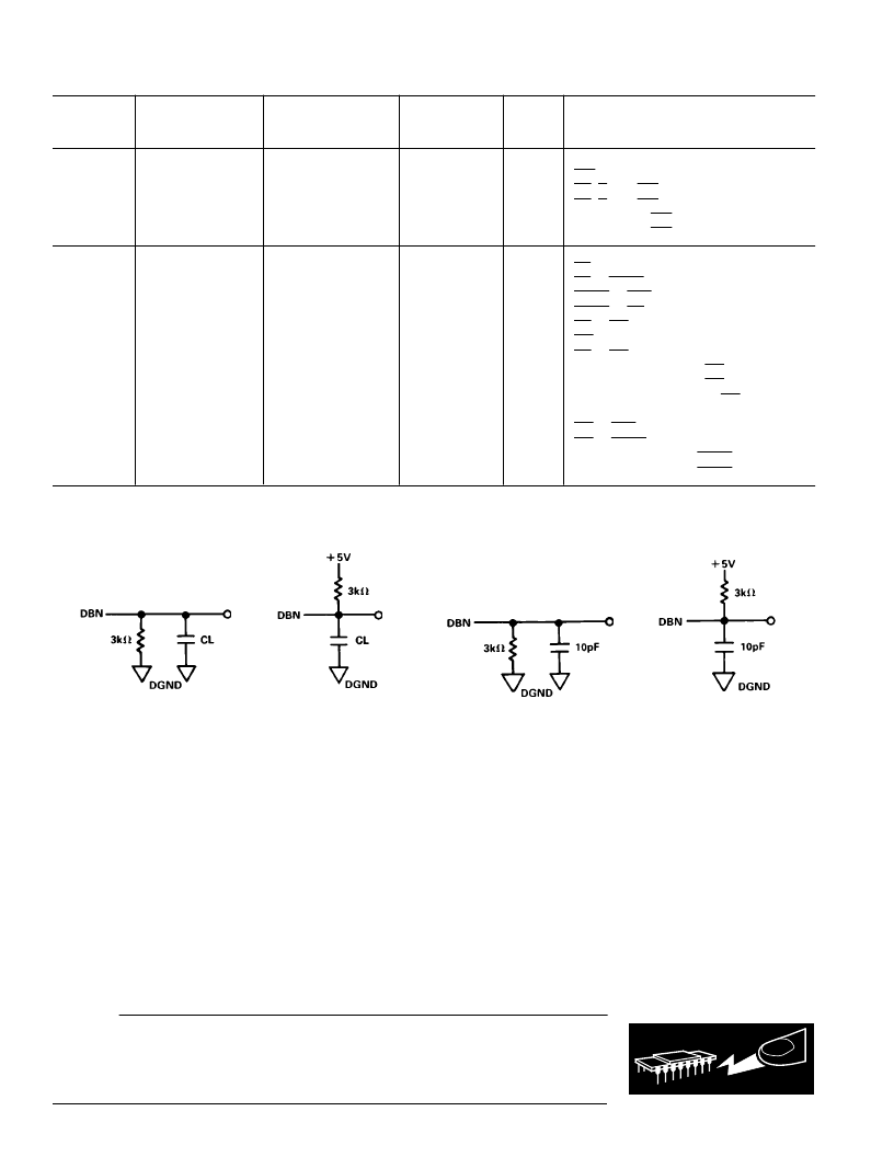
Figure 1. Load Circuits for Data Access Time Test
a. High-Z to V
OH
Figure 2. Load Circuits for Bus Relinquish Time Test
b. High-Z to V
OL
a. V
OH
to High-Z
b. V
OL
to High-Z
Power Dissipation (Any Package) to +75
°
C . . . . . . . . 450 mW
Derates above 75
°
C by . . . . . . . . . . . . . . . . . . . . . 6 mW/
°
C
Operating Temperature Range
Commercial (J, K) . . . . . . . . . . . . . . . . . . . . . . 0
°
C to +70
°
C
Industrial (A, B) . . . . . . . . . . . . . . . . . . . . . –40
°
C to +85
°
C
Extended (S, T) . . . . . . . . . . . . . . . . . . . . –55
°
C to +125
°
C
Storage Temperature Range . . . . . . . . . . . . –65
°
C to +150
°
C
Lead Temperature (Soldering, 10 secs) . . . . . . . . . . . +300
°
C
*Stresses above those listed under “Absolute Maximum Ratings” may cause
permanent damage to the device. This is a stress rating only; functional operation
of the device at these or any other condition above those indicated in the
operational sections of this specification is not implied. Exposure to absolute
maximum rating conditions for extended periods may affect device reliability.
(See Figures 8, 10, 12; V
DD
= 5 V
6
5%; V
SS
= 0 V or –5 V
6
5%)
相關PDF資料 |
PDF描述 |
|---|---|
| AD7569KP | LC2MOS Complete, 8-Bit Analog I/0 Systems |
| AD7569TQ | LC2MOS Complete, 8-Bit Analog I/0 Systems |
| AD7669AR | LC2MOS Complete, 8-Bit Analog I/0 Systems |
| AD7569 | Complete, 8-Bit Analog I/0 Systems(完備的8位模擬I/O系統) |
| AD7669 | Complete, 8-Bit Analog I/0 Systems(完備的8位模擬I/O系統) |
相關代理商/技術參數 |
參數描述 |
|---|---|
| AD7569KNZ | 功能描述:IC I/O PORT 8BIT ANALOG 24DIP RoHS:是 類別:集成電路 (IC) >> 接口 - 專用 系列:LC²MOS 特色產品:NXP - I2C Interface 標準包裝:1 系列:- 應用:2 通道 I²C 多路復用器 接口:I²C,SM 總線 電源電壓:2.3 V ~ 5.5 V 封裝/外殼:16-TSSOP(0.173",4.40mm 寬) 供應商設備封裝:16-TSSOP 包裝:剪切帶 (CT) 安裝類型:表面貼裝 產品目錄頁面:825 (CN2011-ZH PDF) 其它名稱:568-1854-1 |
| AD7569KP | 制造商:Analog Devices 功能描述:Data Acquisition System Single ADC Single DAC 8-Bit 28-Pin PLCC 制造商:Rochester Electronics LLC 功能描述:8-BIT CMOS I/O PORT IC - Bulk |
| AD7569KP-REEL | 制造商:Analog Devices 功能描述:Data Acquisition System Single ADC Single DAC 8-Bit 28-Pin PLCC T/R 制造商:Analog Devices 功能描述:DATA ACQ SYS SGL ADC SGL DAC 8BIT 28PLCC - Tape and Reel 制造商:Rochester Electronics LLC 功能描述:8-BIT CMOS I/O PORT IC - Tape and Reel |
| AD7569KPZ | 制造商:Analog Devices 功能描述:Data Acquisition System Single ADC Single DAC 8-Bit 28-Pin PLCC |
| AD7569SQ | 制造商:Rochester Electronics LLC 功能描述:8-BIT CMOS I/O PORT IC - Bulk |
發布緊急采購,3分鐘左右您將得到回復。