- 您現在的位置:買賣IC網 > PDF目錄373912 > AD7569SE (ANALOG DEVICES INC) LC2MOS Complete, 8-Bit Analog I/0 Systems PDF資料下載
參數資料
| 型號: | AD7569SE |
| 廠商: | ANALOG DEVICES INC |
| 元件分類: | 模擬信號調理 |
| 英文描述: | LC2MOS Complete, 8-Bit Analog I/0 Systems |
| 中文描述: | SPECIALTY ANALOG CIRCUIT, CQCC28 |
| 封裝: | CERAMIC, LCC-28 |
| 文件頁數: | 11/20頁 |
| 文件大小: | 504K |
| 代理商: | AD7569SE |
AD7569/AD7669
–11–
REV. B
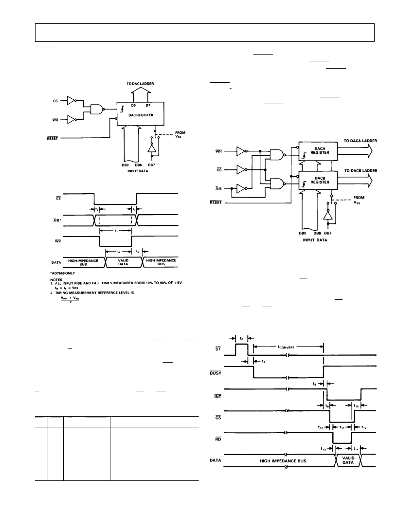
RESET
line, the DAC output resets to 0 V when the entire
system is reset. Figure 7 shows the input control logic for the
AD7569 DAC; the write cycle timing diagram is shown in
Figure 8.
Figure 7. AD7569 DAC Input Control Logic
Figure 8. AD7569/AD7669 Write Cycle Timing Diagram
DAC Timing and Control—AD7669
Table III shows the truth table for the dual DAC operation of
the AD7669. The part contains two 8-bit DAC registers that are
loaded from the data bus under the control of
CS
,
A
/B and
WR
.
Address line
A
/B selects which DAC register the data is
loaded to. The data contained in the DAC registers determines
the analog output from the respective DACs. The
WR
input is
an edge-triggered input, and data is transferred into the selected
DAC register on the rising edge of
WR
. Holding
CS
and
WR
low does not make the selected DAC register transparent. The
A
/B input should not be changed while
CS
and
WR
are low.
Table III. AD7669 DAC Truth Table
CS
WR
A
/B
RESET
DAC Function
H
L
g
L
g
X
H
g
L
g
L
X
X
L
L
H
H
X
H
H
H
H
H
L
DAC Registers Unaffected
DACA Register Updated
DACA Register Updated
DACB Register Updated
DACB Register Updated
DAC Registers Loaded with
All Zeros
L = Low State, H = High State, X = Don’t Care
The contents of the DAC registers are reset to all 0s by an active
low pulse on the
RESET
line, and for the unipolar output
ranges, the outputs remain at 0 V after
RESET
returns high.
For the bipolar output ranges, a low pulse on
RESET
causes the
outputs to go to negative full scale. In unipolar applications, the
RESET
line can be used to ensure power-up to 0 V on the
AD7669 DAC outputs and is also useful when used as a zero
override in system calibration cycles. If the
RESET
input is con-
nected to the system
RESET
line, then the DAC outputs reset
to 0 V when the entire system is reset. Figure 9 shows the DAC
input control logic for the AD7669, and the write cycle timing
diagram is shown in Figure 8.
Figure 9. AD7669 DAC Control Logic
ADC Timing and Control
The ADC on the AD7569/AD7669 is capable of two basic oper-
ating modes. In the first mode, the
ST
line is used to start con-
version and drive the track-and-hold into hold mode. At the end
of conversion, the track-and-hold returns to its tracking mode.
The second mode is achieved by hard-wiring the
ST
line high.
In this case,
CS
and
RD
start conversion, and the microproces-
sor is driven into a WAIT state for the duration of conversion by
BUSY
.
Figure 10. ADC Mode 1 Interface Timing
相關PDF資料 |
PDF描述 |
|---|---|
| AD7569SQ | LC2MOS Complete, 8-Bit Analog I/0 Systems |
| AD7569ACHIPS | LC2MOS Complete, 8-Bit Analog I/0 Systems |
| AD7569JN | LC2MOS Complete, 8-Bit Analog I/0 Systems |
| AD7669JN | LC2MOS Complete, 8-Bit Analog I/0 Systems |
| AD7569JP | LC2MOS Complete, 8-Bit Analog I/0 Systems |
相關代理商/技術參數 |
參數描述 |
|---|---|
| AD7569SQ | 制造商:Rochester Electronics LLC 功能描述:8-BIT CMOS I/O PORT IC - Bulk |
| AD7569SQ/883B | 制造商:Analog Devices 功能描述: |
| AD7569TQ | 制造商:Rochester Electronics LLC 功能描述:- Bulk |
| AD7572, AD7572AAR03 | 制造商: 功能描述: 制造商:undefined 功能描述: |
| AD7572AAN03 | 制造商:Analog Devices 功能描述:ADC Single SAR 12-bit Parallel 24-Pin PDIP 制造商:Rochester Electronics LLC 功能描述:12-BIT ADC IC - Bulk |
發布緊急采購,3分鐘左右您將得到回復。