- 您現在的位置:買賣IC網 > PDF目錄373909 > AD7575SE (ANALOG DEVICES INC) LC2MOS 5 us 8-Bit ADC with Track/Hold PDF資料下載
參數資料
| 型號: | AD7575SE |
| 廠商: | ANALOG DEVICES INC |
| 元件分類: | ADC |
| 英文描述: | LC2MOS 5 us 8-Bit ADC with Track/Hold |
| 中文描述: | 1-CH 8-BIT SUCCESSIVE APPROXIMATION ADC, PARALLEL ACCESS, CQCC20 |
| 封裝: | CERAMIC, LCC-20 |
| 文件頁數: | 8/12頁 |
| 文件大小: | 146K |
| 代理商: | AD7575SE |
AD7575
–8–
REV. B
INTERNAL/EXTERNAL CLOCK
The AD7575 can be used with its own internal clock or with an
externally applied clock. In either case, the clock signal appear-
ing at the CLK pin is divided internally by two to provide an
internal clock signal for the AD7575. A single conversion lasts
for 20 input clock cycles (10 internal clock cycles).
INTERNAL CLOCK
Clock pulses are generated by the action of the external capaci-
tor (C
CLK
) charging through an external resistor (R
CLK
) and
discharging through an internal switch. When a conversion is
complete, the internal clock stops operating. In addition to
conversion, the internal clock also controls the automatic inter-
nal reset of the SAR. This reset occurs at the start of each con-
version cycle during the first internal clock pulse.
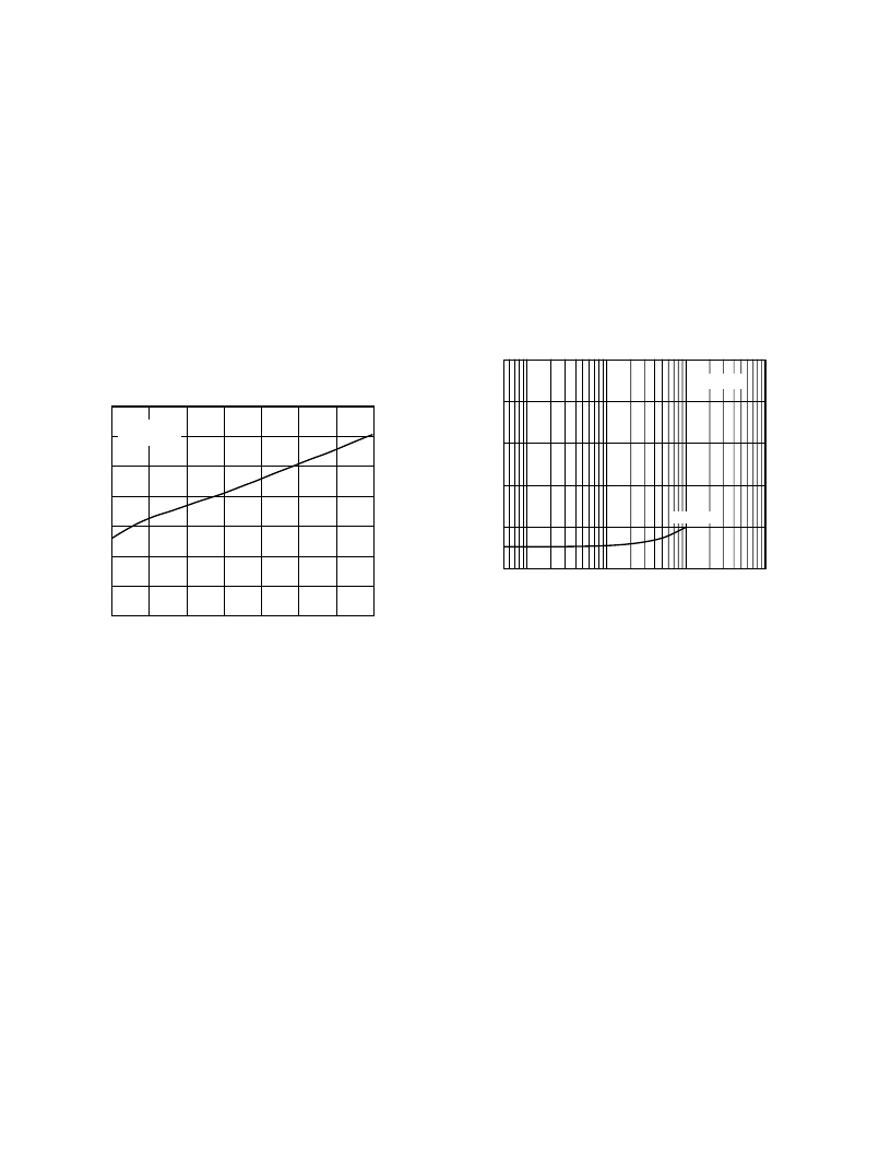
Nominal conversion times versus temperature for the recom-
mended R
CLK
and C
CLK
combination are shown in Figure 13.
AMBIENT TEMPERATURE –
8
C
14
7–55
+125
–25
C
m
s
0
+25
+50
+75
+100
13
11
10
9
8
12
R
CLK
= 100k
V
C
CLK
= 100pF
Figure 13. Typical Conversion Times vs. Temperature
Using Internal Clock
The internal clock is useful because it provides a convenient
clock source for the AD7575. Due to process variations, the
actual operating frequency for this R
CLK
/C
CLK
combination can
vary from device to device by up to
±
50%. For this reason it is
recommended that an external clock be used in the following
situations:
1. Applications requiring a conversion time that is within 50% of
5
μ
s, the minimum conversion time for specified accuracy. A
clock frequency of 4 MHz at the CLK pin gives a conversion
time of 5
μ
s.
2. Applications where time related software constraints cannot
accommodate time differences that may occur due to unit to
unit clock frequency variations or temperature.
EXTERNAL CLOCK
The CLK input of the AD7575 may be driven directly from
74 HC, 4000B series buffers (such as 4049) or from LS TTL
with a 5.6 k
pull-up resistor. When conversion is complete, the
internal clock is disabled even if the external clock is still ap-
plied. This means that the external clock can continue to run
between conversions without being disabled. The mark/space
ratio of the external clock can vary from 70/30 to 30/70.
The AD7575 is specified for operation at a 5
μ
s conversion rate;
with a 4 MHz input clock frequency. If the part is operated at
slower clock frequencies, it may result in slightly degraded accu-
racy performance from the part. This is a result of leakage ef-
fects on the hold capacitor. Figure 14 shows a typical plot of
accuracy versus conversion time for the AD7575.
CONVERSION TIME –
m
s
2.5
5
10000
R
50
500
2.0
1.5
1.0
0.5
0
100
1000
5000
10
T
A
= +25
8
C
AD7575KN
Figure 14. Accuracy vs. Conversion Time
相關PDF資料 |
PDF描述 |
|---|---|
| AD7575SQ | LC2MOS 5 us 8-Bit ADC with Track/Hold |
| AD7575TE | LC2MOS 5 us 8-Bit ADC with Track/Hold |
| AD7575TQ | LC2MOS 5 us 8-Bit ADC with Track/Hold |
| AD7576JN | LC2MOS 10 us uP-Compatible 8-Bit ADC |
| AD7576 | LC2MOS 10 us uP-Compatible 8-Bit ADC |
相關代理商/技術參數 |
參數描述 |
|---|---|
| AD7575TCHIPS | 功能描述:8 Bit Analog to Digital Converter 1 Input 1 SAR Die 制造商:analog devices inc. 系列:- 包裝:托盤 - 晶粒 零件狀態:上次購買時間 位數:8 采樣率(每秒):- 輸入數:1 輸入類型:單端 數據接口:并聯 配置:S/H-ADC 無線電 - S/H:ADC:1:1 A/D 轉換器數:1 架構:SAR 參考類型:外部 電壓 - 電源,模擬:5V 電壓 - 電源,數字:5V 特性:- 工作溫度:-55°C ~ 125°C 封裝/外殼:模具 供應商器件封裝:模具 標準包裝:1 |
| AD7576AQ | 制造商:Rochester Electronics LLC 功能描述:- Bulk 制造商:Analog Devices 功能描述: |
| AD7576BQ | 制造商:Rochester Electronics LLC 功能描述:- Bulk |
| AD7576JN | 制造商:Rochester Electronics LLC 功能描述:- Bulk 制造商:Analog Devices 功能描述:IC 8BIT ADC 7576 DIP18 |
| AD7576JP | 制造商:Rochester Electronics LLC 功能描述:- Bulk |
發布緊急采購,3分鐘左右您將得到回復。