- 您現(xiàn)在的位置:買賣IC網(wǎng) > PDF目錄373911 > AD7628TE (ANALOG DEVICES INC) CMOS Dual 8-Bit Buffered Multiplying DAC PDF資料下載
參數(shù)資料
| 型號: | AD7628TE |
| 廠商: | ANALOG DEVICES INC |
| 元件分類: | DAC |
| 英文描述: | CMOS Dual 8-Bit Buffered Multiplying DAC |
| 中文描述: | DUAL, PARALLEL, 8 BITS INPUT LOADING, 8-BIT DAC, CQCC20 |
| 封裝: | CERAMIC, LCC-20 |
| 文件頁數(shù): | 3/8頁 |
| 文件大小: | 193K |
| 代理商: | AD7628TE |
AD7628
–3–
REV. A
ABSOLUT E MAX IMUM RAT INGS
(T
A
= +25
°
C unless otherwise noted)
V
DD
to AGND . . . . . . . . . . . . . . . . . . . . . . . . . . . . 0 V, +17 V
V
DD
to DGND . . . . . . . . . . . . . . . . . . . . . . . . . . . . 0 V, +17 V
AGND to DGND . . . . . . . . . . . . . . . . . . . . . . . . V
DD
+ 0.3 V
DGND to AGND . . . . . . . . . . . . . . . . . . . . . . . . V
DD
+ 0.3 V
Digital Input Voltage to DGND . . . . . . –0.3 V, V
DD
+ 0.3 V
V
PIN2
, V
PIN20
to AGND . . . . . . . . . . . . . . –0.3 V, V
DD
+ 0.3 V
V
REF
A, V
REF
B to AGND . . . . . . . . . . . . . . . . . . . . . . .
±
25 V
V
RFB
A, V
RFB
B to AGND . . . . . . . . . . . . . . . . . . . . . . .
±
25 V
Power Dissipation (Any Package) to +75
°
C . . . . . . . . 450 mW
Derates above +75
°
C by . . . . . . . . . . . . . . . . . . . 6 mW/
°
C
Operating T emperature Range
Commercial (K ) Grades . . . . . . . . . . . . . . . –40
°
C to +85
°
C
Industrial (B) Grades . . . . . . . . . . . . . . . . . –40
°
C to +85
°
C
Extended (T ) Grades . . . . . . . . . . . . . . . . –55
°
C to +125
°
C
Storage T emperature . . . . . . . . . . . . . . . . . –65
°
C to +150
°
C
Lead T emperature (Soldering, 10 sec) . . . . . . . . . . . . +300
°
C
ORDE RING GUIDE
T emperature
Range
Relative
Accuracy
Gain
E rror
Package
Option
2
Model
1
AD7628K N
AD7628K P
AD7628K R
AD7628BQ
AD7628T Q
AD7628T E
–40
°
C to +85
°
C
–40
°
C to +85
°
C
–40
°
C to +85
°
C
–40
°
C to +85
°
C
–55
°
C to +125
°
C
–55
°
C to +125
°
C
±
1/2 LSB
±
1/2 LSB
±
1/2 LSB
±
1/2 LSB
±
1/2 LSB
±
1/2 LSB
±
2 LSB
±
2 LSB
±
2 LSB
±
2 LSB
±
2 LSB
±
2 LSB
N-20
P-20A
R-20
Q-20
Q-20
E-20A
NOT ES
1
T o order MIL-ST D-883, Class B process parts, add /883B to part number.
Contact your local sales office for military data sheet.
2
E = Leadless Ceramic Chip Carrier; N = Plastic DIP; P = Plastic Leaded Chip
Carrier; Q = Cerdip; R = SOIC.
WARNING!
ESD SENSITIVE DEVICE
C AUT ION
ESD (electrostatic discharge) sensitive device. Electrostatic charges as high as 4000 V readily
accumulate on the human body and test equipment and can discharge without detection.
Although the AD7628 features proprietary ESD protection circuitry, permanent damage may
occur on devices subjected to high energy electrostatic discharges. T herefore, proper ESD
precautions are recommended to avoid performance degradation or loss of functionality.
T E RMINOLOGY
Relative Accuracy:
Relative accuracy or endpoint nonlinearity is a measure of the
maximum deviation from a straight line passing through the
endpoints of the DAC transfer function. It is measured after ad-
justing for zero and full-scale, and is normally expressed in
LSBs or as a percentage of full-scale reading.
Differential Nonlinearity:
Differential nonlinearity is the difference between the measured
change and the ideal 1 LSB change between any two adjacent
codes. A specified differential nonlinearity of
±
1 LSB max over
the operating temperature range ensures monotonicity.
Gain E rror:
Gain error is a measure of the output error between an ideal
DAC and the actual device output. It is measured with all 1s in
the DAC latches after offset error has been adjusted out. Gain
error of both DACs is adjustable to zero with external resistance.
Output Capacitance:
Capacitance from OUT A or OUT B to AGND.
Digital-to-Analog Glitch Impulse:
T he amount of charge injected from the digital inputs to the
analog output when the inputs change state. T his is normally
specified as the area of the glitch in either pA-secs or nV-secs,
depending upon whether the glitch is measured as a current or
voltage signal. Glitch impulse is measured with V
REF
A, V
REF
B
= AGND.
Channel-to-Channel Isolation:
T he proportion of input signal from one DAC’s reference input
that appears at the output of the other DAC, expressed as a
ratio in dB.
Digital Crosstalk:
T he glitch energy transferred to the output of one converter due
to a change in digital input code to the other converter. Speci-
fied in nV secs.
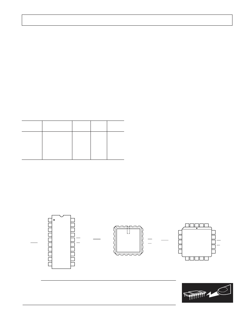
PIN CONFIGURAT IONS
LC C C
DIP, SOIC
AGND
OUT A
OUT B
RFB B
DGND
DAC A/DAC B
(MSB) DB7
WR
CS
DB0 (LSB)
RFB A
V
REF
A
V
REF
B
V
DD
DB6
DB1
DB5
DB2
DB4
DB3
1
2
20
19
5
6
7
16
15
14
3
4
18
17
8
13
9
12
10
11
TOP VIEW
(Not to Scale)
AD7628
V
REF
A
DGND
DB6
DAC A /DAC B
DB7 (MSB)
O
2
R
19
A
1
O
20
D
D
D
D
D
V
REF
B
V
DD
WR
DB0 (LSB)
CS
3
4
5
8
6
7
12 13
9
11
10
18
17
14
16
15
TOP VIEW
(Not to Scale)
AD7628
R
PLC C
V
REF
A
DGND
DB6
DAC A/DAC B
DB7 (MSB)
R
O
R
A
O
D
D
D
D
D
V
REF
B
V
DD
DB0 (LSB)
WR
CS
19
3
1
2
20
4
5
8
6
7
12
13
9
11
10
18
17
14
16
15
TOP VIEW
(Not to Scale)
AD7628
相關(guān)PDF資料 |
PDF描述 |
|---|---|
| AD7628TQ | ECONOLINE: REC2.2-S_DRW(Z)/H* - 2.2W DIP Package- 1kVDC Isolation- Regulated Output- 4.5-9V, 9-18V, 18-36V, 36-72V Wide Input Range 2 : 1- UL94V-0 Package Material- Continuous Short Circiut Protection- Cost Effective- 100% Burned In- Efficiency to 84% |
| AD7631 | 18-Bit 250/670 kSPS PulSAR Bipolar Programmable Inputs ADC |
| AD7634 | 18-Bit 250/670 kSPS PulSAR Bipolar Programmable Inputs ADC |
| AD7641BCPZ | 18-Bit 250/670 kSPS PulSAR Bipolar Programmable Inputs ADC |
| AD7641BCPZRL | 18-Bit 250/670 kSPS PulSAR Bipolar Programmable Inputs ADC |
相關(guān)代理商/技術(shù)參數(shù) |
參數(shù)描述 |
|---|---|
| AD7628TQ | 制造商:Rochester Electronics LLC 功能描述:CMOS DUAL 8 BIT D/A CONVE - Bulk |
| AD7628TQ/883B | 制造商:Analog Devices 功能描述:DAC 2-CH R-2R 8-bit 20-Pin CDIP Tube 制造商:Analog Devices 功能描述:DAC 2CH R-2R 8BIT 20CDIP - Rail/Tube |
| AD7630ACP | 制造商:Analog Devices 功能描述:500KSPS 18-BIT ADC S/W PROG. INPUT RANGES - Bulk |
| AD7630AST | 制造商:Analog Devices 功能描述:500KSPS 18-BIT ADC S/W PROG. INPUT RANGES - Bulk |
| AD7631 | 制造商:AD 制造商全稱:Analog Devices 功能描述:14-Bit, 1 MSPS, Differential, Programmable Input PulSAR ADC |
發(fā)布緊急采購,3分鐘左右您將得到回復。