- 您現在的位置:買賣IC網 > PDF目錄373912 > AD7664ASTRL (ANALOG DEVICES INC) 16-Bit, 570 kSPS CMOS ADC PDF資料下載
參數資料
| 型號: | AD7664ASTRL |
| 廠商: | ANALOG DEVICES INC |
| 元件分類: | ADC |
| 英文描述: | 16-Bit, 570 kSPS CMOS ADC |
| 中文描述: | 1-CH 16-BIT SUCCESSIVE APPROXIMATION ADC, SERIAL/PARALLEL ACCESS, PQFP48 |
| 封裝: | MS-026BBC, LQFP-48 |
| 文件頁數: | 16/19頁 |
| 文件大小: | 392K |
| 代理商: | AD7664ASTRL |
REV. 0
AD7664
–16–
While the AD7664 is performing a bit decision, it is important
that voltage transients not occur on digital input/output pins or
degradation of the conversion result could occur. This is par-
ticularly important during the second half of the conversion
phase because the AD7664 provides error correction circuitry
that can correct for an improper bit decision made during the
first half of the conversion phase. For this reason, it is recom-
mended that when an external clock is being provided, it is a
discontinuous clock that is toggling only when BUSY is low or,
more importantly, that is does not transition during the latter
half of BUSY high.
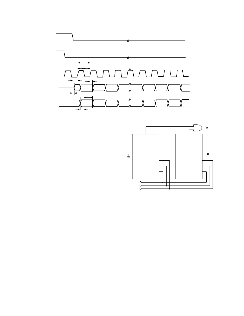
External Discontinuous Clock Data Read After Conversion
Though the maximum throughput cannot be achieved using this
mode, it is the most recommended of the serial slave modes.
Figure 18 shows the detailed timing diagrams of this method.
After a conversion is complete, indicated by BUSY returning
low, the result of this conversion can be read while both
CS
and
RD
are low. The data is shifted out, MSB first, with 16 clock
pulses and is valid on both rising and falling edge of the clock.
Among the advantages of this method, the conversion perfor-
mance is not degraded because there are no voltage transients
on the digital interface during the conversion process.
Another advantage is to be able to read the data at any speed up
to 40 MHz which accommodates both slow digital host interface
and the fastest serial reading.
Finally, in this mode only, the AD7664 provides a “daisy chain”
feature using the RDC/SDIN input pin for cascading multiple
converters together. This feature is useful for reducing component
count and wiring connections when desired as, for instance, in
isolated multiconverter applications.
An example of the concatenation of two devices is shown in
Figure 19. Simultaneous sampling is possible by using a com-
mon
CNVST
signal. It should be noted that the RDC/SDIN
input is latched on the opposite edge of SCLK of the one used to
shift out the data on SDOUT. Hence, the MSB of the “upstream”
converter just follows the LSB of the “downstream” converter
on the next SCLK cycle.
SCLK
SDOUT
D15
D14
D1
D0
D13
X15
X14
X13
X1
X0
Y15
Y14
CS
,
RD
BUSY
SDIN
EXT/I
NT
= 1
INVSCLK = 0
t
35
t
36
t
37
t
31
t
32
t
16
t
33
t
34
X15
X14
X
1
2
3
14
15
16
17
18
Figure 18. Slave Serial Data Timing for Reading (Read After Convert)
CNVST
CS
SCLK
SDOUT
RDC/SDIN
BUSY
BUSY
DATA
OUT
AD7664
#1
(DOWNSTREAM)
BUSY
OUT
CNVST
CS
SCLK
AD7664
#2
(UPSTREAM)
RDC/SDIN
SDOUT
SCLK IN
CS IN
CNVST IN
Figure 19. Two AD7664s in a “Daisy Chain” Configuration
External Clock Data Read During Conversion
Figure 20 shows the detailed timing diagrams of this method.
During a conversion, while both
CS
and
RD
are both low, the
result of the previous conversion can be read. The data is shifted
out, MSB first, with 16 clock pulses and is valid on both rising and
falling edge of the clock. The 16 bits have to be read before the
current conversion is complete. If that is not done, RDERROR is
pulsed high and can be used to interrupt the host interface to
prevent incomplete data reading. There is no “daisy chain”
feature in this mode and RDC/SDIN input should always be
tied either high or low.
To reduce performance degradation due to digital activity, a fast
discontinuous clock of, at least 18 MHz, when impulse mode is
used, 25 MHz when normal mode is used or 40 MHz when warp
mode is used, is recommended to ensure that all the bits are read
during the first half of the conversion phase. It is also possible
to begin to read the data after conversion and continue to read
the last bits even after a new conversion has been initiated. That
allows the use of a slower clock speed like 14 MHz in impulse
mode, 18 MHz in normal mode and 25 MHz in warp mode.
相關PDF資料 |
PDF描述 |
|---|---|
| AD7664AST | 16-Bit, 570 kSPS CMOS ADC |
| AD7665 | TV 8C 8#20 PIN PLUG |
| AD7665AST | 16-Bit, 570 kSPS CMOS ADC |
| AD7665ASTRL | 16-Bit, 570 kSPS CMOS ADC |
| AD7669AN | LC2MOS Complete, 8-Bit Analog I/0 Systems |
相關代理商/技術參數 |
參數描述 |
|---|---|
| AD7664ASTZ | 功能描述:IC ADC 16BIT UNIPOLAR 48-LQFP RoHS:是 類別:集成電路 (IC) >> 數據采集 - 模數轉換器 系列:PulSAR® 標準包裝:1 系列:microPOWER™ 位數:8 采樣率(每秒):1M 數據接口:串行,SPI? 轉換器數目:1 功率耗散(最大):- 電壓電源:模擬和數字 工作溫度:-40°C ~ 125°C 安裝類型:表面貼裝 封裝/外殼:24-VFQFN 裸露焊盤 供應商設備封裝:24-VQFN 裸露焊盤(4x4) 包裝:Digi-Reel® 輸入數目和類型:8 個單端,單極 產品目錄頁面:892 (CN2011-ZH PDF) 其它名稱:296-25851-6 |
| AD7664ASTZRL | 功能描述:IC ADC 16BIT UNIPOLAR 48LQFP RoHS:是 類別:集成電路 (IC) >> 數據采集 - 模數轉換器 系列:PulSAR® 標準包裝:1 系列:- 位數:14 采樣率(每秒):83k 數據接口:串行,并聯 轉換器數目:1 功率耗散(最大):95mW 電壓電源:雙 ± 工作溫度:0°C ~ 70°C 安裝類型:通孔 封裝/外殼:28-DIP(0.600",15.24mm) 供應商設備封裝:28-PDIP 包裝:管件 輸入數目和類型:1 個單端,雙極 |
| AD7664CST | 制造商:未知廠家 制造商全稱:未知廠家 功能描述:Analog to Digital Converter |
| AD7664CSTRL | 制造商:未知廠家 制造商全稱:未知廠家 功能描述:Analog to Digital Converter |
| AD7665 | 制造商:AD 制造商全稱:Analog Devices 功能描述:14-Bit, 1 MSPS, Differential, Programmable Input PulSAR ADC |
發布緊急采購,3分鐘左右您將得到回復。