- 您現在的位置:買賣IC網 > PDF目錄373912 > AD7669AR (ANALOG DEVICES INC) LC2MOS Complete, 8-Bit Analog I/0 Systems PDF資料下載
參數資料
| 型號: | AD7669AR |
| 廠商: | ANALOG DEVICES INC |
| 元件分類: | 模擬信號調理 |
| 英文描述: | LC2MOS Complete, 8-Bit Analog I/0 Systems |
| 中文描述: | SPECIALTY ANALOG CIRCUIT, PDSO28 |
| 封裝: | SOIC-28 |
| 文件頁數: | 16/20頁 |
| 文件大小: | 504K |
| 代理商: | AD7669AR |
–16–
REV. B
AD7569/AD7669
APPLYING THE AD7569/AD7669 ADC
The analog input on the AD7569/AD7669 accepts the same
four input ranges as the output ranges on the DAC. Whatever
output range is selected for the DAC also applies to the input
range of the ADC.
Although separate AGNDs exist for both the DAC and ADC to
minimize crosstalk, writing data to the DAC while the ADC is
performing a conversion may result in an incorrect conversion
from the ADC due to an interaction of currents between the
DAC and ADC. Therefore, to ensure correct operation of the
ADC, the DAC register should not be updated while the ADC
is converting.
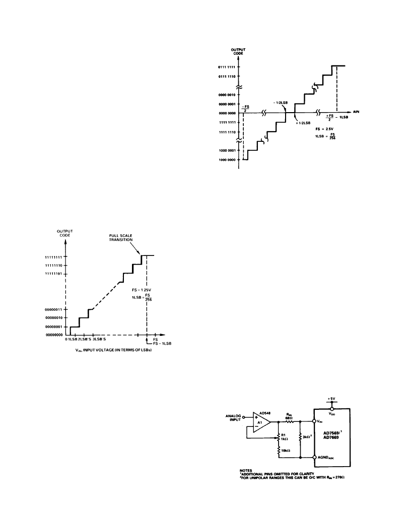
UNIPOLAR OPERATION
The circuit of Figure 21 shows the AD7569 configured for both
an input and output range of 0 V to +1.25 V (the AD7669 con-
figuration is similar). The nominal transfer characteristic for this
range is shown in Figure 22. The output code is Natural Binary
with 1 LSB = (1.25/256)V = 4.88 mV.
As before, to achieve the unipolar 0 V to +2.5 V input range,
V
SS
is connected to 0 V, and the RANGE input is tied to a logic
high. The nominal transfer characteristic is as in Figure 22 but,
in this case, 1 LSB = (2.5/256)V = 9.76 mV.
Figure 22. Nominal Transfer Characteristic for Unipolar
(0 V to +1.25 V) Operation
BIPOLAR OPERATION
The analog input of the AD7569/AD7669 ADC is configured
for bipolar inputs when V
SS
= –5 V. The output code provided
by the part is twos complement. Figure 23 shows the transfer
function for bipolar (–1.25 V to +1.25 V) operation. The LSB
size for this range is (2.5/256)V = 9.76 mV.
The transfer function for the –2.5 V to +2.5 V range is identical
to that of Figure 23, but now FS = 5 V and the LSB size is
(5/256)V = 19.5 mV.
ADC OFFSET AND FULL-SCALE ERROR ADJUSTMENT
In most Digital Signal Processing (DSP) applications, offset and
full-scale error have little or no effect on system performance. A
Figure 23. Nominal Transfer Characteristic for Bipolar
(–1.25 V to +1.25 V) Operation
typical example is a digital filter where an ac analog signal is
quantized by the ADC, digitally processed and recreated using
the DAC. In these types of applications, the offset error can be
eliminated by ac coupling the recreated signal. Full-scale error
effect is linear and does not cause problems as long as the input
signal is within the full dynamic range of the ADC. An impor-
tant parameter in DSP applications is Differential Nonlinearity,
and this is not affected by either offset or full-scale error.
In applications where absolute accuracy is important ADC off-
set and full-scale error can be adjusted to zero. Figure 24 shows
the additional components required for offset and full-scale er-
ror adjustment. Offset error must be adjusted before full-scale
error. Zero offset is achieved by adjusting the offset of the op
amp driving V
IN
(i.e., A1 in Figure 23). In unipolar applica-
tions, for zero offset error, apply 1/2 LSB at the analog input
and adjust the op amp offset voltage until the ADC output code
flickers between 0000 0000 and 0000 0001. For zero full-scale
error, apply an analog input of FS – 3/2 LSBs and adjust R1 un-
til the ADC output code flickers between 1111 1110 and 1111
1111.
In bipolar applications, to adjust for bipolar zero offset, apply
–1/2 LSB at the analog input and adjust the op amp offset volt-
age until the output code flickers between 1111 1111 and 0000
0000. For zero full-scale error, apply +FS/2 – 3/2 LSB at the
analog input and adjust R1 until the ADC output code flickers
between 0111 1110 and 0111 1111.
Figure 24. ADC Error Adjust Circuit
相關PDF資料 |
PDF描述 |
|---|---|
| AD7569 | Complete, 8-Bit Analog I/0 Systems(完備的8位模擬I/O系統) |
| AD7669 | Complete, 8-Bit Analog I/0 Systems(完備的8位模擬I/O系統) |
| AD7569AQ | LC2MOS Complete, 8-Bit Analog I/0 Systems |
| AD7569BN | LC2MOS Complete, 8-Bit Analog I/0 Systems |
| AD7569BQ | LC2MOS Complete, 8-Bit Analog I/0 Systems |
相關代理商/技術參數 |
參數描述 |
|---|---|
| AD7669AR-REEL | 制造商:Analog Devices 功能描述: |
| AD7669ARZ | 功能描述:IC I/O PORT 8BIT ANALOG 28SOIC RoHS:是 類別:集成電路 (IC) >> 接口 - 專用 系列:LC²MOS 特色產品:NXP - I2C Interface 標準包裝:1 系列:- 應用:2 通道 I²C 多路復用器 接口:I²C,SM 總線 電源電壓:2.3 V ~ 5.5 V 封裝/外殼:16-TSSOP(0.173",4.40mm 寬) 供應商設備封裝:16-TSSOP 包裝:剪切帶 (CT) 安裝類型:表面貼裝 產品目錄頁面:825 (CN2011-ZH PDF) 其它名稱:568-1854-1 |
| AD7669ARZ-REEL | 功能描述:IC I/O PORT 8BIT ANALOG 28SOIC RoHS:是 類別:集成電路 (IC) >> 接口 - 專用 系列:LC²MOS 特色產品:NXP - I2C Interface 標準包裝:1 系列:- 應用:2 通道 I²C 多路復用器 接口:I²C,SM 總線 電源電壓:2.3 V ~ 5.5 V 封裝/外殼:16-TSSOP(0.173",4.40mm 寬) 供應商設備封裝:16-TSSOP 包裝:剪切帶 (CT) 安裝類型:表面貼裝 產品目錄頁面:825 (CN2011-ZH PDF) 其它名稱:568-1854-1 |
| AD7669JN | 制造商:Analog Devices 功能描述:Data Acquisition System Single ADC Dual DAC 8-Bit 28-Pin PDIP W 制造商:Rochester Electronics LLC 功能描述:COMPLETE 8 BIT I/O SYSTEM - Bulk |
| AD7669JNZ | 功能描述:IC I/O PORT 8BIT ANLG 28DIP RoHS:是 類別:集成電路 (IC) >> 接口 - 專用 系列:LC²MOS 特色產品:NXP - I2C Interface 標準包裝:1 系列:- 應用:2 通道 I²C 多路復用器 接口:I²C,SM 總線 電源電壓:2.3 V ~ 5.5 V 封裝/外殼:16-TSSOP(0.173",4.40mm 寬) 供應商設備封裝:16-TSSOP 包裝:剪切帶 (CT) 安裝類型:表面貼裝 產品目錄頁面:825 (CN2011-ZH PDF) 其它名稱:568-1854-1 |
發布緊急采購,3分鐘左右您將得到回復。