- 您現在的位置:買賣IC網 > PDF目錄373912 > AD7669JR (ANALOG DEVICES INC) LC2MOS Complete, 8-Bit Analog I/0 Systems PDF資料下載
參數資料
| 型號: | AD7669JR |
| 廠商: | ANALOG DEVICES INC |
| 元件分類: | 模擬信號調理 |
| 英文描述: | LC2MOS Complete, 8-Bit Analog I/0 Systems |
| 中文描述: | SPECIALTY ANALOG CIRCUIT, PDSO24 |
| 封裝: | SOIC-24 |
| 文件頁數: | 3/20頁 |
| 文件大小: | 504K |
| 代理商: | AD7669JR |
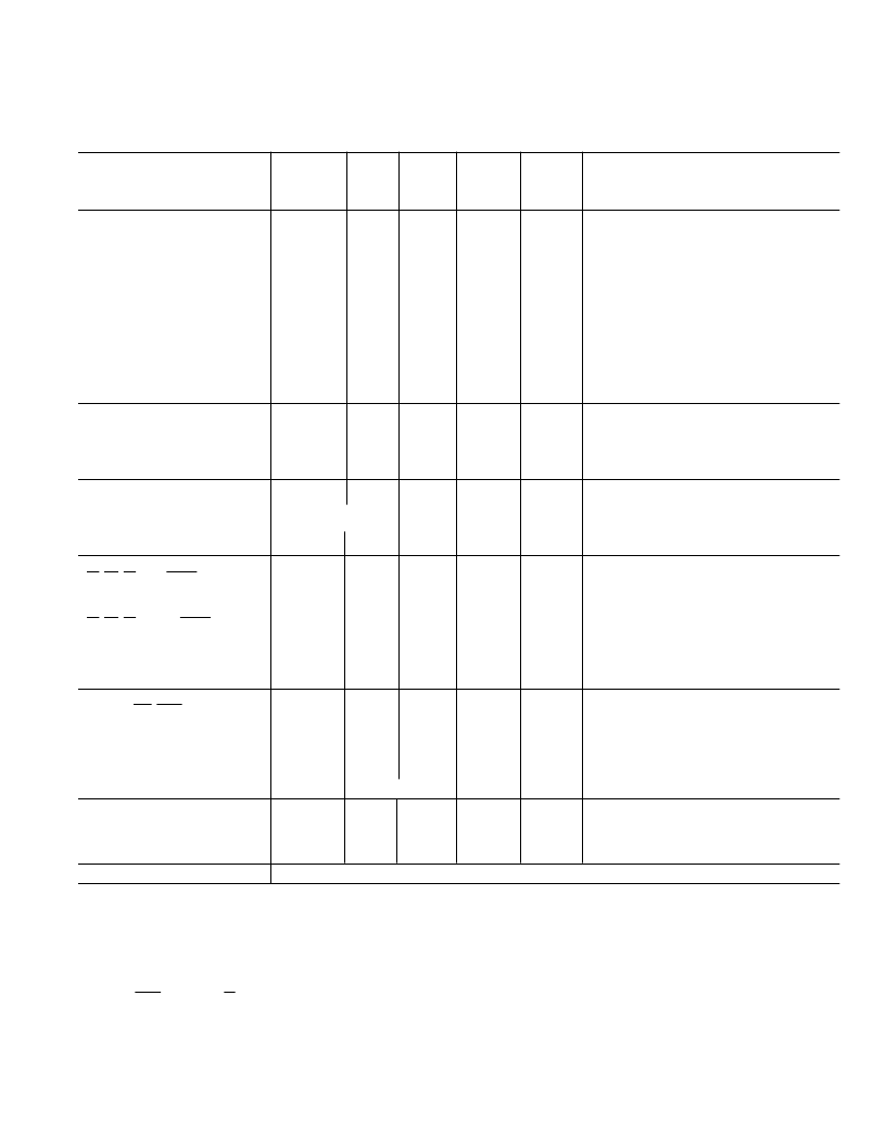
ADC SPECIFICATIONS
wise noted. All specifications T
MIN
to T
MAX
unless otherwise noted.) Specifications apply to Mode 1 interface.
AD7569
J, A Versions
3
AD7669
J Version
AD7569
K, B
Versions
AD7569
S Version
AD7569
T Version
Parameter
Units
Conditions/Comments
DC ACCURACY
Resolution
3
Total Unadjusted Error
4
Relative Accuracy
4
Differential Nonlinearity
4
Unipolar Offset Error
@ +25
°
C
T
to T
Bipolar Zero Offset Error
@ +25
°
C
T
MIN
to T
MAX
Full-Scale Error
5
@ +25
°
C
T
to T
MAX
Full Scale/
DD
, T
A
= +25
°
C
Full Scale/
V
SS
, T
A
= +25
°
C
8
±
3
±
1
±
1
8
±
3
±
1/2
±
3/4
8
±
4
±
1
±
1
8
±
4
±
1/2
±
3/4
Bits
LSB typ
LSB max
LSB max
No Missing Codes
Typical tempco is 10
μ
V/
°
C for +1.25 V range; V
SS
= 0 V
±
2
±
3
±
1.5
±
2.5
±
2
±
3
±
1.5
±
2.5
LSB max
LSB max
Typical tempco is 20
μ
V/
°
C for + 1.25 V range; V
SS
= –5 V
±
3
±
3.5
±
2.5
±
3
±
3
±
4
±
2.5
±
3.5
LSB max
LSB max
V
DD
= 5 V
–4, +0
–5.5, +1.5
0.5
0.5
–4, +0
–5.5, +1.5
0.5
0.5
–4, +0
–7.5, +2
0.5
0.5
–4, +0
–7.5, +2
0.5
0.5
LSB max
LSB max
LSB max
LSB max
V
IN
= +2.5 V;
V
DD
=
±
5%
V
IN
= –2.5 V;
V
SS
=
±
5%
DYNAMIC PERFORMANCE
Signal-to-Noise Ratio
(SNR)
Total Harmonic Distortion
4
(THD)
Intermodulation Distortion
4
(IMD)
Frequency Response
Track/Hold Acquisition Time
7
44
48
60
0.1
200
46
48
60
0.1
200
44
48
60
0.1
300
45
48
60
0.1
300
dB min
dB max
dB typ
dB typ
ns typ
V
IN
= 100 kHz full-scale sine wave with f
SAMPLING
= 400 kHz
6
V
IN
= 100 kHz full-scale sine wave with f
SAMPLING
= 400 kHz
6
fa = 99 kHz, fb = 96.7 kHz with f
SAMPLING
= 400 kHz
V
IN
=
±
2.5 V, dc to 200 kHz sine wave
ANALOG INPUT
Input Voltage Ranges
Unipolar
Bipolar
Input Current
Input Capacitance
0 to +1.25/ +2.5
±
1.25/
±
2.5
Volts
Volts
μ
A max
pF typ
V
DD
= +5 V; V
SS
= 0 V
V
DD
= +5 V; V
SS
= –5 V
See equivalent circuit Figure 5
±
300
10
±
300
10
±
300
10
±
300
10
LOGIC INPUTS
CS
,
RD
,
ST
, CLK,
RESET
, RANGE
Input Low Voltage, V
INL
Input High Voltage, V
INH
Input Capacitance
8
CS
,
RD
,
ST
, RANGE,
RESET
Input Leakage Current
CLK
Input Current
I
INL
I
INH
0.8
2.4
10
0.8
2.4
10
0.8
2.4
10
0.8
2.4
10
V max
V min
pF max
10
10
10
10
μ
A max
V
IN
= 0 to V
DD
–1.6
40
–1.6
40
–1.6
40
–1.6
40
mA max
μ
A max
V
IN
= 0 V
V
IN
= V
DD
LOGIC OUTPUTS
DB0–DB7,
INT
,
BUSY
V
OL
, Output Low Voltage
V
OH
, Output High Voltage
DB0–DB7
Floating State Leakage Current
Floating State Output Capacitance
8
Output Coding (Single Supply)
Output Coding (Dual Supply)
0.4
4.0
0.4
4.0
0.4
4.0
0.4
4.0
V max
V min
I
SINK
= 1.6 mA
I
SOURCE
= 200
μ
A
10
10
10
10
Binary
2s Complement
10
10
10
10
μ
A max
pF max
CONVERSION TIME
With External Clock
With Internal Clock, T
A
= +25
°
C
2
1.6
2.6
2
1.6
2.6
2
1.6
2.6
2
1.6
2.6
μ
s max
μ
s min
μ
s max
f
CLK
= 5 MHz
Using recommended clock components shown in Figure 21.
Clock frequency can be adjusted by varying R
CLK
.
POWER REQUIREMENTS
As per DAC Specifications
NOTES
1
Except where noted, specifications apply for all ranges including bipolar ranges with dual supply operation.
2
Temperature ranges are as follows: J, K versions; 0
°
C to +70
°
C
A, B versions; –40
°
C to +85
°
C
S, T versions; –55
°
C to +125
°
C
3
1 LSB = 4.88 mV for 0 V to +1.25 V range, 9.76 mV for 0 V to +2.5 V and
±
1.25 V ranges and 19.5 mV for +2.5 V range.
4
See Terminology.
5
Includes internal voltage reference error and is calculated after offset error has been adjusted out. Ideal unipolar last code transition occurs at (FS – 3/2 LSB). Ideal bipolar last code transition occurs at
(FS/2 – 3/2 LSB).
6
Exact frequencies are 101 kHz and 384 kHz to avoid harmonics coinciding with sampling frequency.
7
Rising edge of
BUSY
to falling edge of
ST
. The time given refers to the acquisition time, which gives a 3 dB degradation in SNR from the tested figure.
8
Sample tested at +25
°
C to ensure compliance.
Specifications subject to change without notice.
(V
DD
= +5 V
6
5%; V
SS1
= RANGE = AGND
DAC
= AGND
DAC
= DGND = 0 V; f
CLK
= 5 MHz external unless other-
AD7569/AD7669
–3–
REV. B
相關PDF資料 |
PDF描述 |
|---|---|
| AD7672CQ05 | LC2MOS HIGH-SPEED 12-BIT ADC |
| AD7672CQ10 | LC2MOS HIGH-SPEED 12-BIT ADC |
| AD7672TE05 | LC2MOS HIGH-SPEED 12-BIT ADC |
| AD7672TE10 | LC2MOS HIGH-SPEED 12-BIT ADC |
| AD7672TQ05 | LC2MOS HIGH-SPEED 12-BIT ADC |
相關代理商/技術參數 |
參數描述 |
|---|---|
| AD7669JR-REEL | 制造商:Rochester Electronics LLC 功能描述:- Tape and Reel |
| AD7669JRZ | 功能描述:IC I/O PORT 8BIT ANLG 28SOIC RoHS:是 類別:集成電路 (IC) >> 接口 - 專用 系列:LC²MOS 特色產品:NXP - I2C Interface 標準包裝:1 系列:- 應用:2 通道 I²C 多路復用器 接口:I²C,SM 總線 電源電壓:2.3 V ~ 5.5 V 封裝/外殼:16-TSSOP(0.173",4.40mm 寬) 供應商設備封裝:16-TSSOP 包裝:剪切帶 (CT) 安裝類型:表面貼裝 產品目錄頁面:825 (CN2011-ZH PDF) 其它名稱:568-1854-1 |
| AD7669JRZ-REEL | 功能描述:IC I/O PORT 8BIT ANLG 28SOIC RoHS:是 類別:集成電路 (IC) >> 接口 - 專用 系列:LC²MOS 特色產品:NXP - I2C Interface 標準包裝:1 系列:- 應用:2 通道 I²C 多路復用器 接口:I²C,SM 總線 電源電壓:2.3 V ~ 5.5 V 封裝/外殼:16-TSSOP(0.173",4.40mm 寬) 供應商設備封裝:16-TSSOP 包裝:剪切帶 (CT) 安裝類型:表面貼裝 產品目錄頁面:825 (CN2011-ZH PDF) 其它名稱:568-1854-1 |
| AD766AN | 功能描述:IC DAC 16BIT W/REF DSP 16-DIP RoHS:否 類別:集成電路 (IC) >> 數據采集 - 數模轉換器 系列:DACPORT® 產品培訓模塊:Data Converter Fundamentals DAC Architectures 標準包裝:750 系列:- 設置時間:7µs 位數:16 數據接口:并聯 轉換器數目:1 電壓電源:雙 ± 功率耗散(最大):100mW 工作溫度:0°C ~ 70°C 安裝類型:表面貼裝 封裝/外殼:28-LCC(J 形引線) 供應商設備封裝:28-PLCC(11.51x11.51) 包裝:帶卷 (TR) 輸出數目和類型:1 電壓,單極;1 電壓,雙極 采樣率(每秒):143k |
| AD766ANZ | 功能描述:IC DAC 16BIT W/REF DSP 16-DIP RoHS:是 類別:集成電路 (IC) >> 數據采集 - 數模轉換器 系列:DACPORT® 標準包裝:1 系列:- 設置時間:4.5µs 位數:12 數據接口:串行,SPI? 轉換器數目:1 電壓電源:單電源 功率耗散(最大):- 工作溫度:-40°C ~ 125°C 安裝類型:表面貼裝 封裝/外殼:8-SOIC(0.154",3.90mm 寬) 供應商設備封裝:8-SOICN 包裝:剪切帶 (CT) 輸出數目和類型:1 電壓,單極;1 電壓,雙極 采樣率(每秒):* 其它名稱:MCP4921T-E/SNCTMCP4921T-E/SNRCTMCP4921T-E/SNRCT-ND |
發布緊急采購,3分鐘左右您將得到回復。