- 您現在的位置:買賣IC網 > PDF目錄373913 > AD7694ARM (ANALOG DEVICES INC) 16-Bit, 250 kSPS PulSAR ADC in MSOP PDF資料下載
參數資料
| 型號: | AD7694ARM |
| 廠商: | ANALOG DEVICES INC |
| 元件分類: | ADC |
| 英文描述: | 16-Bit, 250 kSPS PulSAR ADC in MSOP |
| 中文描述: | 1-CH 16-BIT SUCCESSIVE APPROXIMATION ADC, SERIAL ACCESS, PDSO8 |
| 封裝: | MSOP-8 |
| 文件頁數: | 14/16頁 |
| 文件大小: | 281K |
| 代理商: | AD7694ARM |
AD7694
Table 9. Recommended Driver Amplifiers
Amplifier
Typical Application
AD8021
Very low noise and high frequency
AD8022
Low noise and high frequency
OP184
Low power, low noise, and low frequency
AD8605
,
AD8615
5 V single-supply and low power
AD8519
Small, low power, and low frequency
AD8031
High frequency and low power
Rev. 0 | Page 14 of 16
VOLTAGE REFERENCE INPUT
The AD7694 voltage reference input, REF, has a dynamic input
impedance and should therefore be driven by a low impedance
source with efficient decoupling between the REF and GND
pins, as explained in the Layout section.
When REF is driven by a very low impedance source (e.g., an
unbuffered reference voltage like the low temperature drift
ADR43x
reference or a reference buffer using the
AD8031
or
the
AD8605
), a 10 μF (X5R, 0805 size) ceramic chip capacitor is
appropriate for optimum performance.
If desired, smaller reference decoupling capacitor values down
to 2.2 μF can be used with a minimal impact on performance,
especially DNL.
POWER SUPPLY
The AD7694 powers down automatically at the end of each
conversion phase and, therefore, the power scales linearly with
the sampling rate, as shown in Figure 22. This makes the part
ideal for a low sampling rate (even a few Hz) and low battery-
powered applications.
10,000
1,000
100
10
1
0.1
0.01
10
100
1k
10k
100k
1M
0
SAMPLING RATE (SPS)
O
μ
A
VDD = 5V
VDD = 2.7V
Figure 22. Operating Current vs. Sampling Rate
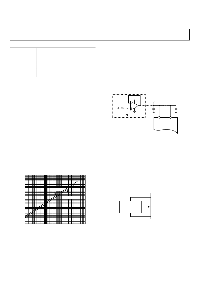
SUPPLYING THE ADC FROM THE REFERENCE
For simplified applications, the AD7694, with its low operating
current, can be supplied directly using the reference circuit, as
shown in Figure 23. The reference line can be driven by either
The system power supply directly
A reference voltage with enough current output capability,
such as the
ADR43x
A reference buffer, such as the
AD8031
, that can also filter
the system power supply, as shown in Figure 23
0
AD8031
AD7694
REF
VDD
2.2
TO
10
μ
F
1
μ
F
10
10k
5V OR 3V
5V
OR
3V
5V OR 3V
1
μ
F
(NOTE 1)
NOTE 1: OPTIONAL REFERENCE BUFFER AND FILTER
Figure 23. Example of an Application Circuit
DIGITAL INTERFACE
The AD7694 is compatible with SPI, QSPI, digital hosts, and
DSPs, e.g., Blackfin ADSP-BF53x or ADSP-219x. The connec-
tion diagram is shown in Figure 24 and the corresponding
timing diagram is shown in Figure 25.
A rising edge on CNV initiates a conversion and forces SDO to
high impedance. When the conversion is complete, the AD7694
enters the acquisition phase and powers down. When CNV goes
low, the MSB is output onto SDO. The remaining data bits are
then clocked by subsequent SCK falling edges. The data is valid
on both SCK edges.
0
CNV
SCK
SDO
DATA IN
CLK
CONVERT
DIGITAL HOST
AD7694
Figure 24. Connection Diagram
相關PDF資料 |
PDF描述 |
|---|---|
| AD7694ARMRL7 | 16-Bit, 250 kSPS PulSAR ADC in MSOP |
| AD7694BRM | 16-Bit, 250 kSPS PulSAR ADC in MSOP |
| AD7694BRMRL7 | 16-Bit, 250 kSPS PulSAR ADC in MSOP |
| AD7701AN | LC2MOS 16-Bit A/D Converter |
| AD7701AQ | LC2MOS 16-Bit A/D Converter |
相關代理商/技術參數 |
參數描述 |
|---|---|
| AD7694ARMRL7 | 制造商:AD 制造商全稱:Analog Devices 功能描述:16-Bit, 250 kSPS PulSAR ADC in MSOP |
| AD7694ARMZ | 功能描述:IC ADC 16BIT SAR 250KSPS 8MSOP RoHS:是 類別:集成電路 (IC) >> 數據采集 - 模數轉換器 系列:PulSAR® 標準包裝:1,000 系列:- 位數:12 采樣率(每秒):300k 數據接口:并聯 轉換器數目:1 功率耗散(最大):75mW 電壓電源:單電源 工作溫度:0°C ~ 70°C 安裝類型:表面貼裝 封裝/外殼:24-SOIC(0.295",7.50mm 寬) 供應商設備封裝:24-SOIC 包裝:帶卷 (TR) 輸入數目和類型:1 個單端,單極;1 個單端,雙極 |
| AD7694ARMZRL7 | 功能描述:IC ADC 16BIT SAR 250KSPS 8-MSOP RoHS:是 類別:集成電路 (IC) >> 數據采集 - 模數轉換器 系列:PulSAR® 標準包裝:1,000 系列:- 位數:16 采樣率(每秒):45k 數據接口:串行 轉換器數目:2 功率耗散(最大):315mW 電壓電源:模擬和數字 工作溫度:0°C ~ 70°C 安裝類型:表面貼裝 封裝/外殼:28-SOIC(0.295",7.50mm 寬) 供應商設備封裝:28-SOIC W 包裝:帶卷 (TR) 輸入數目和類型:2 個單端,單極 |
| AD7694BRM | 制造商:Rochester Electronics LLC 功能描述: 制造商:Analog Devices 功能描述: |
| AD7694BRMRL7 | 制造商:Rochester Electronics LLC 功能描述: 制造商:Analog Devices 功能描述: |
發布緊急采購,3分鐘左右您將得到回復。