- 您現(xiàn)在的位置:買賣IC網(wǎng) > PDF目錄373913 > AD7694ARMRL7 (ANALOG DEVICES INC) 16-Bit, 250 kSPS PulSAR ADC in MSOP PDF資料下載
參數(shù)資料
| 型號(hào): | AD7694ARMRL7 |
| 廠商: | ANALOG DEVICES INC |
| 元件分類: | ADC |
| 英文描述: | 16-Bit, 250 kSPS PulSAR ADC in MSOP |
| 中文描述: | 1-CH 16-BIT SUCCESSIVE APPROXIMATION ADC, SERIAL ACCESS, PDSO8 |
| 封裝: | MSOP-8 |
| 文件頁(yè)數(shù): | 13/16頁(yè) |
| 文件大小: | 281K |
| 代理商: | AD7694ARMRL7 |
第1頁(yè)第2頁(yè)第3頁(yè)第4頁(yè)第5頁(yè)第6頁(yè)第7頁(yè)第8頁(yè)第9頁(yè)第10頁(yè)第11頁(yè)第12頁(yè)當(dāng)前第13頁(yè)第14頁(yè)第15頁(yè)第16頁(yè)
AD7694
Rev. 0 | Page 13 of 16
0
AD7694
REF
GND
VDD
IN–
IN+
SCK
SDO
CNV
3-WIRE INTERFACE
100nF
2.7V TO 5.25V
2.2 TO 10
μ
F
(NOTE 2)
REF
0 TO V
REF
33
2.7nF
(NOTE 3)
(NOTE 4)
(NOTE 1)
NOTE 1: SEE REFERENCE SECTION FOR REFERENCE SELECTION.
NOTE 2: C
IS USUALLY A 10
μ
F CERAMIC CAPACITOR (X5R).
NOTE 3: SEE DRIVER AMPLIFIER CHOICE SECTION.
NOTE 4. OPTIONAL FILTER. SEE ANALOG INPUT SECTION.
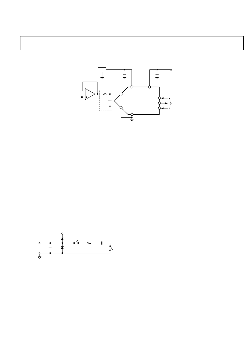
Figure 20. Typical Application Diagram
TYPICAL CONNECTION DIAGRAM
Figure 20 shows an example of the recommended application
diagram for the AD7694.
ANALOG INPUT
Figure 21 shows an equivalent circuit of the AD7694 input
structure. The two diodes, D1 and D2, provide ESD protection
for the analog inputs, IN+ and IN. Care must be taken to
ensure that the analog input signal never exceeds the supply
rails by more than 0.3 V, because this will cause these diodes to
become forward-biased and start conducting current. However,
these diodes can handle a forward-biased current of 130 mA,
maximum. For instance, these conditions could eventually
occur when the input buffer’s (U1) supplies are different from
VDD. In such a case, an input buffer with a short-circuit current
limitation can be used to protect the part.
0
C
IN
R
IN
D1
D2
C
PIN
IN+
OR IN–
GND
VDD
Figure 21. Equivalent Analog Input Circuit
This analog input structure allows the sampling of the
differential signal between IN+ and IN. By using this
differential input, small signals common to both inputs are
rejected. For instance, by using IN to sense a remote signal
ground, ground potential differences between the sensor and
the local ADC ground are eliminated. During the acquisition
phase, the impedance of the analog input IN+ can be modeled
as a parallel combination of the capacitor C
PIN
and the network
formed by the series connection of R
IN
and C
IN
. C
PIN
is primarily
the pin capacitance. R
IN
is typically 600 and is a lumped
component made up of some serial resistors and the on-
resistance of the switches. C
IN
is typically 30 pF and is mainly
the ADC sampling capacitor. During the conversion phase,
where the switches are opened, the input impedance is limited
to C
PIN
. R
IN
and C
IN
make a 1-pole, low-pass filter that reduces
undesirable aliasing effects and limits the noise.
When the source impedance of the driving circuit is low, the
AD7694 can be driven directly. Large source impedances
significantly affect the ac performance, especially total
harmonic distortion (THD). The dc performances are less
sensitive to the input impedance.
DRIVER AMPLIFIER CHOICE
Although the AD7694 is easy to drive, the driver amplifier
needs to meet the following requirements:
The noise generated by the driver amplifier needs to be
kept as low as possible in order to preserve the SNR and
transition noise performance of the AD7694. Note that the
AD7694 has a noise much lower than most of the other
16-bit ADCs and, therefore, can be driven by a noisier op
amp while preserving the same or better system perfor-
mance. The noise coming from the driver is filtered by the
AD7694 analog input circuit 1-pole, low-pass filter made
by R1 and C2 or by the external filter, if one is used.
For ac applications, the driver needs to have a THD
performance suitable to that of the AD7694. Figure 13
gives the THD versus frequency that the driver
should exceed.
For multichannel multiplexed applications, the driver
amplifier and the AD7694 analog input circuit must be able
to settle for a full-scale step of the capacitor array at a
16-bit level (0.0015%). In the amplifier’s data sheet, settling
at 0.1% to 0.01% is more commonly specified. This could
differ significantly from the settling time at a 16-bit level
and should be verified prior to driver selection.
相關(guān)PDF資料 |
PDF描述 |
|---|---|
| AD7694BRM | 16-Bit, 250 kSPS PulSAR ADC in MSOP |
| AD7694BRMRL7 | 16-Bit, 250 kSPS PulSAR ADC in MSOP |
| AD7701AN | LC2MOS 16-Bit A/D Converter |
| AD7701AQ | LC2MOS 16-Bit A/D Converter |
| AD7701AR | LC2MOS 16-Bit A/D Converter |
相關(guān)代理商/技術(shù)參數(shù) |
參數(shù)描述 |
|---|---|
| AD7694ARMZ | 功能描述:IC ADC 16BIT SAR 250KSPS 8MSOP RoHS:是 類別:集成電路 (IC) >> 數(shù)據(jù)采集 - 模數(shù)轉(zhuǎn)換器 系列:PulSAR® 標(biāo)準(zhǔn)包裝:1,000 系列:- 位數(shù):12 采樣率(每秒):300k 數(shù)據(jù)接口:并聯(lián) 轉(zhuǎn)換器數(shù)目:1 功率耗散(最大):75mW 電壓電源:單電源 工作溫度:0°C ~ 70°C 安裝類型:表面貼裝 封裝/外殼:24-SOIC(0.295",7.50mm 寬) 供應(yīng)商設(shè)備封裝:24-SOIC 包裝:帶卷 (TR) 輸入數(shù)目和類型:1 個(gè)單端,單極;1 個(gè)單端,雙極 |
| AD7694ARMZRL7 | 功能描述:IC ADC 16BIT SAR 250KSPS 8-MSOP RoHS:是 類別:集成電路 (IC) >> 數(shù)據(jù)采集 - 模數(shù)轉(zhuǎn)換器 系列:PulSAR® 標(biāo)準(zhǔn)包裝:1,000 系列:- 位數(shù):16 采樣率(每秒):45k 數(shù)據(jù)接口:串行 轉(zhuǎn)換器數(shù)目:2 功率耗散(最大):315mW 電壓電源:模擬和數(shù)字 工作溫度:0°C ~ 70°C 安裝類型:表面貼裝 封裝/外殼:28-SOIC(0.295",7.50mm 寬) 供應(yīng)商設(shè)備封裝:28-SOIC W 包裝:帶卷 (TR) 輸入數(shù)目和類型:2 個(gè)單端,單極 |
| AD7694BRM | 制造商:Rochester Electronics LLC 功能描述: 制造商:Analog Devices 功能描述: |
| AD7694BRMRL7 | 制造商:Rochester Electronics LLC 功能描述: 制造商:Analog Devices 功能描述: |
| AD7694BRMZ | 功能描述:IC ADC 16BIT SRL 250KSPS 8MSOP RoHS:是 類別:集成電路 (IC) >> 數(shù)據(jù)采集 - 模數(shù)轉(zhuǎn)換器 系列:PulSAR® 其它有關(guān)文件:TSA1204 View All Specifications 標(biāo)準(zhǔn)包裝:1 系列:- 位數(shù):12 采樣率(每秒):20M 數(shù)據(jù)接口:并聯(lián) 轉(zhuǎn)換器數(shù)目:2 功率耗散(最大):155mW 電壓電源:模擬和數(shù)字 工作溫度:-40°C ~ 85°C 安裝類型:表面貼裝 封裝/外殼:48-TQFP 供應(yīng)商設(shè)備封裝:48-TQFP(7x7) 包裝:Digi-Reel® 輸入數(shù)目和類型:4 個(gè)單端,單極;2 個(gè)差分,單極 產(chǎn)品目錄頁(yè)面:1156 (CN2011-ZH PDF) 其它名稱:497-5435-6 |
發(fā)布緊急采購(gòu),3分鐘左右您將得到回復(fù)。