- 您現在的位置:買賣IC網 > PDF目錄373913 > AD7703AR (ANALOG DEVICES INC) LC2MOS 20-Bit A/D Converter PDF資料下載
參數資料
| 型號: | AD7703AR |
| 廠商: | ANALOG DEVICES INC |
| 元件分類: | ADC |
| 英文描述: | LC2MOS 20-Bit A/D Converter |
| 中文描述: | 1-CH 20-BIT DELTA-SIGMA ADC, SERIAL ACCESS, PDSO20 |
| 封裝: | MS-013AC, SOIC-20 |
| 文件頁數: | 3/16頁 |
| 文件大小: | 251K |
| 代理商: | AD7703AR |
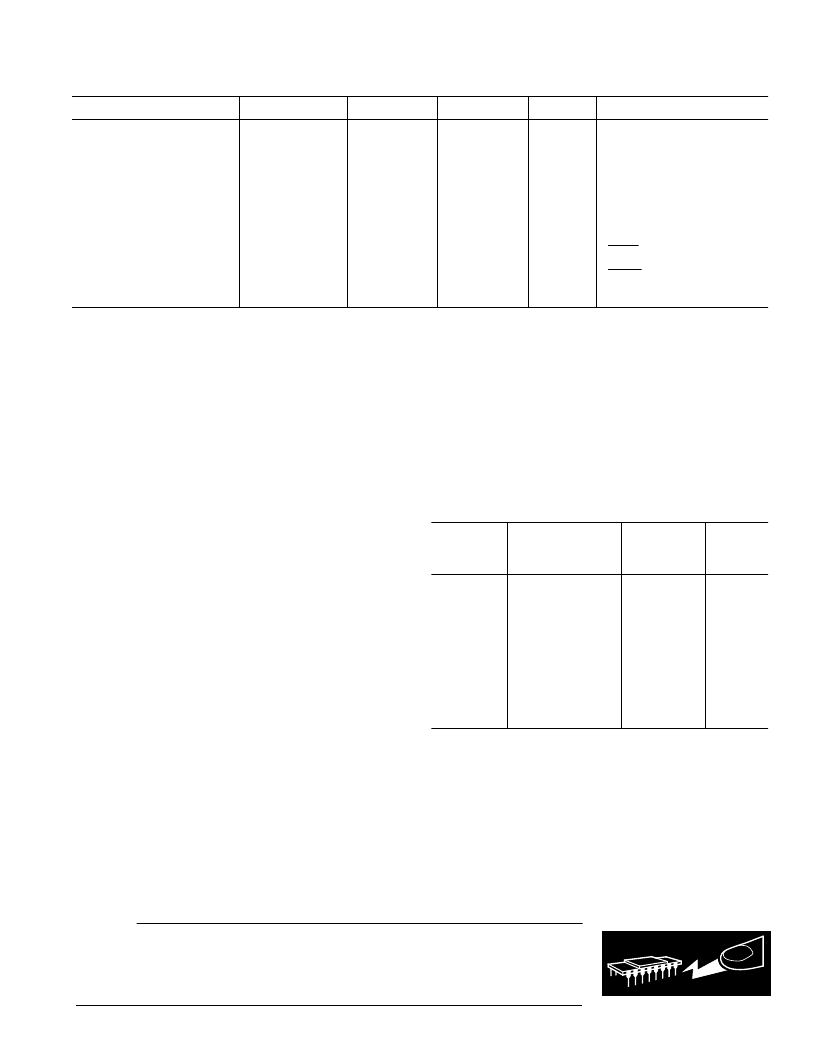
Parameter
A/S Versions
2
B Version
2
C Version
2
Units
T est Conditions/Comments
ST AT IC PERFORMANCE
DC Power Supply Currents
8
Analog Positive Supply (AI
DD
)
Digital Positive Supply (DI
DD
)
Analog Negative Supply (AI
SS
)
Digital Negative Supply (DI
SS
)
Power Supply Rejection
Positive Supplies
Negative Supplies
Power Dissipation
Normal Operation
3.2
1.5
3.2
0.1
3.2
1.5
3.2
0.1
3.2
1.5
3.2
0.1
mA max
mA max
mA max
mA max
T ypically 2 mA
T ypically 1 mA
T ypically 2 mA
T ypically 0.03 mA
70
75
70
75
70
75
dB typ
dB typ
40
40
40
mW rnax
SLEEP
= Logic 1,
T ypically 25 mW
SLEEP
= Logic 0,
T ypically 10
μ
W
Standby Operations
10
A, B, C
S
20
40
20
40
20
40
μ
W max
μ
W max
NOT ES
1
T he A
pin presents a very high impedance dynamic load which varies with clock frequency. A ceramic 1 nF capacitor from the A
IN
to AGND is necessary. Source
resistance should be 750
or less.
2
T emperature Ranges are as follows: A, B, C Versions: –40
°
C to +85
°
C; S Version: –55
°
C to +125
°
C.
3
Applies after calibration at the temperature of interest. Full-Scale Error applies for both unipolar and bipolar input ranges.
4
T otal drift over the specified temperature range after calibration at power-up at +25
°
C. T his is guaranteed by design and/or characterization. Recalibration at any
temperature will remove these errors.
5
In unipolar mode the offset can have a negative value (–V
) such that the unipolar mode can mimic bipolar mode operation.
6
T he specifications for input overrange and for input span apply additional constraints on the offset calibration range.
7
For unipolar mode, input span is the difference between full scale and zero scale. For bipolar mode, input span is the difference between positive and negative
full-scale points. When using less than the maximum input span, the span range may be placed anywhere within the range of
±
(V
REF
+ 0.1).
8
All digital outputs unloaded. All digital inputs at 5 V CMOS levels.
9
Applies in 0.1 Hz to 10 Hz bandwidth. PSRR at 60 Hz will exceed 120 dB due to the digital filter.
10
CLK IN is stopped. All digital inputs are grounded.
Specifications subject to change without notice.
ABSOLUT E MAX IMUM RAT INGS*
(T
A
= +25
°
C unless otherwise noted)
DV
DD
to AGND . . . . . . . . . . . . . . . . . . . . . . . –0.3 V to +6 V
DV
DD
to AV
DD
. . . . . . . . . . . . . . . . . . . . . . .–0.3 V to +0.3 V
DV
SS
to AGND . . . . . . . . . . . . . . . . . . . . . . . . +0.3 V to –6 V
AV
DD
to AGND . . . . . . . . . . . . . . . . . . . . . . . . –0.3 V to +6 V
AV
SS
to AGND . . . . . . . . . . . . . . . . . . . . . . . . +0.3 V to –6 V
AGND to DGND . . . . . . . . . . . . . . . . . . . . .–0.3 V to +0.3 V
Digital Input Voltage to DGND . . . . –0.3 V to DV
DD
+ 0.3 V
Analog Input Voltage to AGND . . . . . . . . . . .AV
SS
– 0.3 V to
. . . . . . . . . . . . . . . . . . . . . . . . . . . . . . . . . . . . . . AV
DD
+ 0.3 V
Input Current to Any Pin Except Supplies
1
. . . . . . . .
±
10 mA
Operating T emperature Range
Industrial (A, B, C Versions) . . . . . . . . . . . –40
°
C to +85
°
C
Extended (S Version) . . . . . . . . . . . . . . . . –55
°
C to +125
°
C
Storage T emperature Range . . . . . . . . . . . . –65
°
C to +150
°
C
Lead T emperature (Soldering, 10 secs) . . . . . . . . . . . +300
°
C
Power Dissipation (DIP Package) to +75
°
C . . . . . . . 450 mW
Derates above +75
°
C by . . . . . . . . . . . . . . . . . . . . 10 mW/
°
C
Power Dissipation (SOIC Package) to +75
°
C . . . . . . 250 mW
Derates above +75
°
C by . . . . . . . . . . . . . . . . . . . . 15 mW/
°
C
NOT ES
*Stresses above those listed under “Absolute Maximum Ratings” may cause
permanent damage to the device. T his is a stress rating only and functional
operation of the device at these or any other conditions above those listed in the
operational sections of this specification is not implied. Exposure to absolute
maximum rating conditions for extended periods may affect device reliability.
1
T ransient currents of up to 100 mA will not cause SCR latch-up.
ORDE RING GUIDE
Linearity
E rror
(% FSR)
T emperature
Range
Package
Options*
Model
AD7703AN
AD7703BN
AD7703CN
AD7703AR
AD7703BR
AD7703CR
AD7703AQ
AD7703BQ
AD7703CQ
AD7703SQ
–40
°
C to +85
°
C
–40
°
C to +85
°
C
–40
°
C to +85
°
C
–40
°
C to +85
°
C
–40
°
C to +85
°
C
–40
°
C to +85
°
C
–40
°
C to +85
°
C
–40
°
C to +85
°
C
–40
°
C to +85
°
C
–55
°
C to +125
°
C
0.003
0.0015
0.0012
0.003
0.0015
0.0012
0.003
0.0015
0.0012
0.003
N-20
N-20
N-20
R-20
R-20
R-20
Q-20
Q-20
Q-20
Q-20
*N = Plastic DIP; R = SOIC; Q = Cerdip.
WARNING!
ESD SENSITIVE DEVICE
C AUT ION
ESD (electrostatic discharge) sensitive device. Electrostatic charges as high as 4000 V readily
accumulate on the human body and test equipment and can discharge without detection.
Although this device features proprietary ESD protection circuitry, permanent damage may
occur on devices subjected to high energy electrostatic discharges. T herefore, proper ESD
precautions are recommended to avoid performance degradation or loss of functionality.
–3–
AD7703
REV. D
相關PDF資料 |
PDF描述 |
|---|---|
| AD7703BN | LC2MOS 20-Bit A/D Converter |
| AD7703BQ | LC2MOS 20-Bit A/D Converter |
| AD7703BR | ECONOLINE: REC2.2-S_DRW(Z)/H* - 2.2W DIP Package- 1kVDC Isolation- Regulated Output- 4.5-9V, 9-18V, 18-36V, 36-72V Wide Input Range 2 : 1- UL94V-0 Package Material- Continuous Short Circiut Protection- Cost Effective- 100% Burned In- Efficiency to 84% |
| AD7703CN | LC2MOS 20-Bit A/D Converter |
| AD7703CQ | LC2MOS 20-Bit A/D Converter |
相關代理商/技術參數 |
參數描述 |
|---|---|
| AD7703AR-REEL | 功能描述:IC ADC 20BIT LC2MOS MONO 20-SOIC RoHS:否 類別:集成電路 (IC) >> 數據采集 - 模數轉換器 系列:- 標準包裝:1 系列:- 位數:14 采樣率(每秒):83k 數據接口:串行,并聯 轉換器數目:1 功率耗散(最大):95mW 電壓電源:雙 ± 工作溫度:0°C ~ 70°C 安裝類型:通孔 封裝/外殼:28-DIP(0.600",15.24mm) 供應商設備封裝:28-PDIP 包裝:管件 輸入數目和類型:1 個單端,雙極 |
| AD7703ARZ | 功能描述:IC ADC 20BIT LC2MOS 20-SOIC RoHS:是 類別:集成電路 (IC) >> 數據采集 - 模數轉換器 系列:- 標準包裝:1 系列:- 位數:14 采樣率(每秒):83k 數據接口:串行,并聯 轉換器數目:1 功率耗散(最大):95mW 電壓電源:雙 ± 工作溫度:0°C ~ 70°C 安裝類型:通孔 封裝/外殼:28-DIP(0.600",15.24mm) 供應商設備封裝:28-PDIP 包裝:管件 輸入數目和類型:1 個單端,雙極 |
| AD7703BN | 功能描述:IC ADC 20BIT LC2MOS 20-DIP RoHS:否 類別:集成電路 (IC) >> 數據采集 - 模數轉換器 系列:- 產品培訓模塊:Lead (SnPb) Finish for COTS Obsolescence Mitigation Program 標準包裝:2,500 系列:- 位數:12 采樣率(每秒):3M 數據接口:- 轉換器數目:- 功率耗散(最大):- 電壓電源:- 工作溫度:- 安裝類型:表面貼裝 封裝/外殼:SOT-23-6 供應商設備封裝:SOT-23-6 包裝:帶卷 (TR) 輸入數目和類型:- |
| AD7703BNZ | 功能描述:IC ADC 20BIT LC2MOS MONO 20DIP RoHS:是 類別:集成電路 (IC) >> 數據采集 - 模數轉換器 系列:- 其它有關文件:TSA1204 View All Specifications 標準包裝:1 系列:- 位數:12 采樣率(每秒):20M 數據接口:并聯 轉換器數目:2 功率耗散(最大):155mW 電壓電源:模擬和數字 工作溫度:-40°C ~ 85°C 安裝類型:表面貼裝 封裝/外殼:48-TQFP 供應商設備封裝:48-TQFP(7x7) 包裝:Digi-Reel® 輸入數目和類型:4 個單端,單極;2 個差分,單極 產品目錄頁面:1156 (CN2011-ZH PDF) 其它名稱:497-5435-6 |
| AD7703BQ | 制造商:AD 制造商全稱:Analog Devices 功能描述:LC2MOS 20-Bit A/D Converter |
發布緊急采購,3分鐘左右您將得到回復。