- 您現(xiàn)在的位置:買賣IC網(wǎng) > PDF目錄373913 > AD7703CQ (ANALOG DEVICES INC) LC2MOS 20-Bit A/D Converter PDF資料下載
參數(shù)資料
| 型號(hào): | AD7703CQ |
| 廠商: | ANALOG DEVICES INC |
| 元件分類: | ADC |
| 英文描述: | LC2MOS 20-Bit A/D Converter |
| 中文描述: | 1-CH 20-BIT DELTA-SIGMA ADC, SERIAL ACCESS, CDIP20 |
| 封裝: | CERDIP-20 |
| 文件頁(yè)數(shù): | 10/16頁(yè) |
| 文件大小: | 251K |
| 代理商: | AD7703CQ |
第1頁(yè)第2頁(yè)第3頁(yè)第4頁(yè)第5頁(yè)第6頁(yè)第7頁(yè)第8頁(yè)第9頁(yè)當(dāng)前第10頁(yè)第11頁(yè)第12頁(yè)第13頁(yè)第14頁(yè)第15頁(yè)第16頁(yè)
AD7703
–10–
REV. D
Initiating Calibration
T able III illustrates the calibration modes available in the
AD7703. Not shown in the table is the function of the BP/
UP
pin which determines whether the converter has been calibrated
to measure bipolar or unipolar signals. A calibration step is
initiated by bringing the CAL pin high for at least 4 CLK IN
cycles and then bringing it low again. T he states of SC1 and
SC2 along with the BP/
UP
pin will determine the type of
calibration to be performed. All three signals should be stable
before the CAL pin is taken positive. T he SC1 and SC2 inputs
are latched when CAL goes high. T he BP/
UP
input is not
latched and therefore must remain in a fixed state throughout
the calibration and measurement cycles. Any time the state of
the BP/
UP
is changed, a new calibration cycle must be
performed to enable the AD7703 to function properly in the
new mode.
When a calibration step is initiated, the
DRDY
signal will go
high and remain high until the step is finished. T able III shows
the number of clock cycles each calibration requires. Once a
calibration step is initiated it must finish before a new calibra-
tion step can be executed. In the two step system calibration
mode, the offset calibration step must be initiated before initiat-
ing the gain calibration step.
T able IV. Output Code Size After Calibration
1 LSB
UNIPOLAR
CAL MODE
ZE RO-SCALE
GAIN FACT OR
BIPOLAR
Self-Cal
V
AGND
V
REF
(
V
REF
±
V
AGND
)
1048576
2(
V
REF
±
V
AGND
)
1048576
System Cal
S
OFF
S
GAIN
(
S
GAIN
±
S
OFF
)
1048576
2(
S
GAIN
±
S
OFF
)
1048576
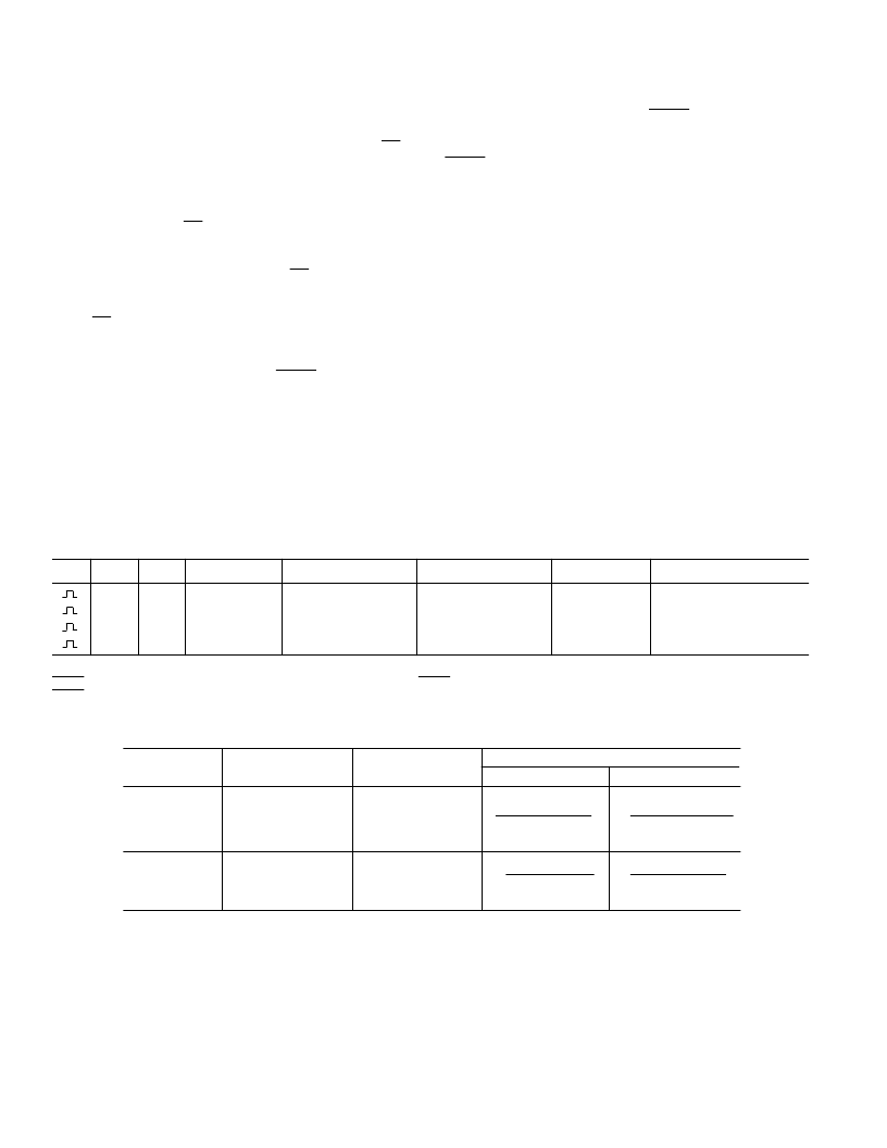
T able III. Calibration T ruth T able
CAL
SC1
SC2
CAL T YPE
ZE RO-SCALE CAL
FULL-SCALE CAL
SE QUE NCE
CALIBRAT ION T IME
0
1
0
1
0
1
1
0
Self-Cal
System Offset
System Gain
System Offset
V
AGND
A
IN
_
A
IN
V
REF
_
A
IN
V
REF
One Step
1st Step
2nd Step
One Step
3,145,655 Clock Cycles
1,052,599 Clock Cycles
1,068,813 Clock Cycles
2,117,389 Clock Cycles
NOT E
DRDY
remains high throughout the calibration sequence. In the Self-Cal mode,
DRDY
falls once the AD7703 has settled to the analog input. In all other modes
DRDY
falls as the device begins to settle.
When self-calibration is completed,
DRDY
falls and the output
port is updated with a data word that represents the analog
input signal. When a system calibration step is completed,
DRDY
will fall and the output port will be updated with the
appropriate data value (all 0s for the zero-scale point and all 1s
for the full-scale point). In the system calibration mode, the
digital filter must settle before the output code will represent the
value of the analog input signal. T ables IV and V indicate the
output code size and output coding of the AD7703 in its
various modes. In these tables, S
OFF
is the measured system
offset in volts and S
GAIN
is the measured system gain at the
full-scale point in volts.
Span and Offset Limits
Whenever a system calibration mode is used, there are limits on
the amount of offset and span which can be accommodated.
T he range of input span in both the unipolar and bipolar modes
has a minimum value of 0.8 V
REF
and a maximum value of
2 (V
REF
+ 0.1 V).
T he amount of offset which can be accommodated depends on
whether the unipolar or bipolar mode is being used. In unipolar
mode, the system calibration modes can handle a maximum
offset of 0.2 V
REF
and a minimum offset of –(V
REF
+ 0.1 V).
T hus the AD7703 in the unipolar mode can be calibrated to
mimic bipolar operation.
相關(guān)PDF資料 |
PDF描述 |
|---|---|
| AD7703CR | ECONOLINE: REC2.2-S_DRW(Z)/H* - 2.2W DIP Package- 1kVDC Isolation- Regulated Output- 4.5-9V, 9-18V, 18-36V, 36-72V Wide Input Range 2 : 1- UL94V-0 Package Material- Continuous Short Circiut Protection- Cost Effective- 100% Burned In- Efficiency to 84% |
| AD7703SQ | LC2MOS 20-Bit A/D Converter |
| AD7705 | 3 V/5 V, 1 mW 2-/3-Channel 16-Bit, Sigma-Delta ADCs |
| AD7705BN | ECONOLINE: REC2.2-S_DR/H1 - 2.2W DIP Package- 1kVDC Isolation- Regulated Output- UL94V-0 Package Material- Continuous Short Circiut Protection- Internal SMD design- 100% Burned In- Efficiency to 75% |
| AD7705BR | ECONOLINE: REC2.2-S_DRW(Z)/H* - 2.2W DIP Package- 1kVDC Isolation- Regulated Output- 4.5-9V, 9-18V, 18-36V, 36-72V Wide Input Range 2 : 1- UL94V-0 Package Material- Continuous Short Circiut Protection- Cost Effective- 100% Burned In- Efficiency to 84% |
相關(guān)代理商/技術(shù)參數(shù) |
參數(shù)描述 |
|---|---|
| AD7703CR | 功能描述:IC ADC 20BIT LC2MOS MONO 20-SOIC RoHS:否 類別:集成電路 (IC) >> 數(shù)據(jù)采集 - 模數(shù)轉(zhuǎn)換器 系列:- 標(biāo)準(zhǔn)包裝:1 系列:- 位數(shù):14 采樣率(每秒):83k 數(shù)據(jù)接口:串行,并聯(lián) 轉(zhuǎn)換器數(shù)目:1 功率耗散(最大):95mW 電壓電源:雙 ± 工作溫度:0°C ~ 70°C 安裝類型:通孔 封裝/外殼:28-DIP(0.600",15.24mm) 供應(yīng)商設(shè)備封裝:28-PDIP 包裝:管件 輸入數(shù)目和類型:1 個(gè)單端,雙極 |
| AD7703CR-REEL | 功能描述:IC ADC 20BIT LC2MOS MONO 20-SOIC RoHS:否 類別:集成電路 (IC) >> 數(shù)據(jù)采集 - 模數(shù)轉(zhuǎn)換器 系列:- 標(biāo)準(zhǔn)包裝:1 系列:- 位數(shù):14 采樣率(每秒):83k 數(shù)據(jù)接口:串行,并聯(lián) 轉(zhuǎn)換器數(shù)目:1 功率耗散(最大):95mW 電壓電源:雙 ± 工作溫度:0°C ~ 70°C 安裝類型:通孔 封裝/外殼:28-DIP(0.600",15.24mm) 供應(yīng)商設(shè)備封裝:28-PDIP 包裝:管件 輸入數(shù)目和類型:1 個(gè)單端,雙極 |
| AD7703CRZ | 功能描述:IC ADC 20BIT LC2MOS MONO 20SOIC RoHS:是 類別:集成電路 (IC) >> 數(shù)據(jù)采集 - 模數(shù)轉(zhuǎn)換器 系列:- 標(biāo)準(zhǔn)包裝:1 系列:- 位數(shù):14 采樣率(每秒):83k 數(shù)據(jù)接口:串行,并聯(lián) 轉(zhuǎn)換器數(shù)目:1 功率耗散(最大):95mW 電壓電源:雙 ± 工作溫度:0°C ~ 70°C 安裝類型:通孔 封裝/外殼:28-DIP(0.600",15.24mm) 供應(yīng)商設(shè)備封裝:28-PDIP 包裝:管件 輸入數(shù)目和類型:1 個(gè)單端,雙極 |
| AD7703SQ | 制造商:AD 制造商全稱:Analog Devices 功能描述:LC2MOS 20-Bit A/D Converter |
| AD7705 | 制造商:AD 制造商全稱:Analog Devices 功能描述:3 V/5 V, 1 mW 2-/3-Channel 16-Bit, Sigma-Delta ADCs |
發(fā)布緊急采購(gòu),3分鐘左右您將得到回復(fù)。