- 您現在的位置:買賣IC網 > PDF目錄373913 > AD7706 (Analog Devices, Inc.) 3 V/5 V, 1 mW 2-/3-Channel 16-Bit, Sigma-Delta ADCs PDF資料下載
參數資料
| 型號: | AD7706 |
| 廠商: | Analog Devices, Inc. |
| 英文描述: | 3 V/5 V, 1 mW 2-/3-Channel 16-Bit, Sigma-Delta ADCs |
| 中文描述: | 3伏/ 5伏,1毫瓦2-/3-Channel 16位Σ-Δ模數轉換器 |
| 文件頁數: | 20/32頁 |
| 文件大小: | 264K |
| 代理商: | AD7706 |
第1頁第2頁第3頁第4頁第5頁第6頁第7頁第8頁第9頁第10頁第11頁第12頁第13頁第14頁第15頁第16頁第17頁第18頁第19頁當前第20頁第21頁第22頁第23頁第24頁第25頁第26頁第27頁第28頁第29頁第30頁第31頁第32頁
AD7705/AD7706
–20–
REV. A
range and the top of its input range) has to take into account the
limitation on the positive full-scale voltage. The amount of
offset which can be accommodated depends on whether the
unipolar or bipolar mode is being used. Once again, the offset
has to take into account the limitation on the positive full-scale
voltage. In unipolar mode, there is considerable flexibility in
handling negative (with respect to AIN(–) on the AD7705 and
with respect to COMMON on the AD7706) offsets. In both
unipolar and bipolar modes, the range of positive offsets that
can be handled by the part depends on the selected span. There-
fore, in determining the limits for system zero-scale and full-
scale calibrations, the user has to ensure that the offset range
plus the span range does exceed 1.05
×
V
REF
/GAIN. This is best
illustrated by looking at a few examples.
If the part is used in unipolar mode with a required span of
0.8
×
V
REF
/GAIN, the offset range the system calibration can
handle is from –1.05
×
V
REF
/GAIN to +0.25
×
V
REF
/GAIN. If
the part is used in unipolar mode with a required span of V
REF
/
GAIN, the offset range the system calibration can handle is
from –1.05
×
V
REF
/GAIN to +0.05
×
V
REF
/GAIN. Similarly, if
the part is used in unipolar mode and required to remove an
offset of 0.2
×
V
REF
/GAIN, the span range the system calibration
can handle is 0.85
×
V
REF
/GAIN.
AD7705/AD7706
INPUT RANGE
(0.8
3
V
REF
/GAIN TO
2.1
3
V
REF
/GAIN)
UPPER LIMIT ON
AD7705 INPUT VOLTAGE
NOMINAL ZERO
SCALE POINT
OFFSET CALIBRATIONS MOVE
INPUT RANGE UP OR DOWN
LOWER LIMIT ON
AD7705/AD7706 INPUT VOLTAGE
–1.05
3
V
REF
/GAIN
–0V DIFFERENTIAL
GAIN CALIBRATIONS EXPAND
OR CONTRACT THE
AD7705/AD7706 INPUT RANGE
1.05
3
V
REF
/GAIN
Figure 13. Span and Offset Limits
If the part is used in bipolar mode with a required span of
±
0.4
×
V
REF
/GAIN, the offset range the system calibration can
handle is from –0.65
×
V
REF
/GAIN to +0.65
×
V
REF
/GAIN.
If the part is used in bipolar mode with a required span of
±
V
REF
/GAIN, then the offset range which the system calibration
can handle is from –0.05
×
V
REF
/GAIN to +0.05
×
V
REF
/GAIN.
Similarly, if the part is used in bipolar mode and required to
remove an offset of
±
0.2
×
V
REF
/GAIN, the span range the sys-
tem calibration can handle is
±
0.85
×
V
REF
/GAIN.
Power-Up and Calibration
On power-up, the AD7705/AD7706 performs an internal reset
that sets the contents of the internal registers to a known state.
There are default values loaded to all registers after power-on or
reset. The default values contain nominal calibration coefficients
for the calibration registers. However, to ensure correct calibra-
tion for the device, a calibration routine should be performed
after power-up.
The power dissipation and temperature drift of the AD7705/
AD7706 are low and no warm-up time is required before the
initial calibration is performed. However, if an external refer-
ence is being used, this reference must have stabilized before
calibration is initiated. Similarly, if the clock source for the part
is generated from a crystal or resonator across the MCLK pins,
the start-up time for the oscillator circuit should elapse before a
calibration is initiated on the part (see below).
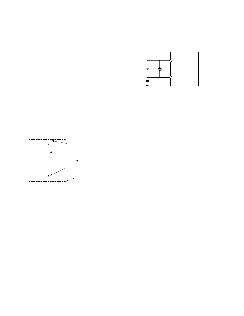
MCLK IN
MCLK OUT
CRYSTAL OR
CERAMIC
RESONATOR
C1
C2
AD7705/AD7706
Figure 14. Crystal/Resonator Connection for the
AD7705/AD7706
USING THE AD7705/AD7706
Clocking and Oscillator Circuit
The AD7705/AD7706 requires a master clock input, which
may be an external CMOS compatible clock signal applied to
the MCLKIN pin with the MCLKOUT pin left unconnected.
Alternatively, a crystal or ceramic resonator of the correct fre-
quency can be connected between MCLKIN and MCLKOUT
as shown in figure 6, in which case the clock circuit will function
as an oscillator, providing the clock source for the part. The
input sampling frequency, the modulator sampling frequency,
the –3dB frequency, output update rate and calibration time
are all directly related to the master clock frequency, f
CLKIN
.
Reducing the master clock frequency by a factor of 2 will halve
the above frequencies and update rate and double the calibra-
tion time. The current drawn from the V
DD
power supply is also
related to f
CLKIN
. Reducing f
CLKIN
by a factor of 2 will halve the
digital part of the total V
DD
current but will not affect the cur-
rent drawn by the analog circuitry.
Using the part with a crystal or ceramic resonator between the
MCLK IN and MCLK OUT pins generally causes more cur-
rent to be drawn from V
DD
than when the part is clocked from
a driven clock signal at the MCLK IN pin. This is because the
on-chip oscillator circuit is active in the case of the crystal or
ceramic resonator. Therefore, the lowest possible current on
the AD7705/AD7706 is achieved with an externally applied
clock at the MCLK IN pin with MCLK OUT unconnected,
unloaded and disabled.
The amount of additional current taken by the oscillator de-
pends on a number of factors—first, the larger the value of
capacitor (C1 and C2) placed on the MCLKIN and MCLKOUT
pins, the larger the current consumption on the AD7705/
AD7706. Care should be taken not to exceed the capacitor
values recommended by the crystal and ceramic resonator
manufacturers to avoid consuming unnecessary current. Typical
values for C1 and C2 are recommended by crystal or ceramic
resonator manufacturers, these are in the range of 30pF to
50pF and if the capacitor values on MCLK IN and MCLK
OUT are kept in this range they will not result in any excessive
current. Another factor that influences the current is the effec-
tive series resistance (ESR) of the crystal that appears between
the MCLK IN and MCLK OUT pins of the AD7705/AD7706.
As a general rule, the lower the ESR value the lower the current
taken by the oscillator circuit.
相關PDF資料 |
PDF描述 |
|---|---|
| AD7706BN | ECONOLINE: REC2.2-S_DRW(Z)/H* - 2.2W DIP Package- 1kVDC Isolation- Regulated Output- 4.5-9V, 9-18V, 18-36V, 36-72V Wide Input Range 2 : 1- UL94V-0 Package Material- Continuous Short Circiut Protection- Cost Effective- 100% Burned In- Efficiency to 84% |
| AD7706BR | 3 V/5 V, 1 mW 2-/3-Channel 16-Bit, Sigma-Delta ADCs |
| AD7706BRU | 3 V/5 V, 1 mW 2-/3-Channel 16-Bit, Sigma-Delta ADCs |
| AD7705EB | Precision Zero-Drift Operational Amplifier with Internal Capacitors; Package: SO; No of Pins: 8; Temperature Range: 0°C to +70°C |
| AD7706* | 3 V/5 V. 1 mW 2-/3-Channel 16-Bit. Sigma-Delta ADCs |
相關代理商/技術參數 |
參數描述 |
|---|---|
| AD7706BN | 功能描述:IC ADC 16BIT 3CH 16-DIP RoHS:否 類別:集成電路 (IC) >> 數據采集 - 模數轉換器 系列:- 產品培訓模塊:Lead (SnPb) Finish for COTS Obsolescence Mitigation Program 標準包裝:2,500 系列:- 位數:12 采樣率(每秒):3M 數據接口:- 轉換器數目:- 功率耗散(最大):- 電壓電源:- 工作溫度:- 安裝類型:表面貼裝 封裝/外殼:SOT-23-6 供應商設備封裝:SOT-23-6 包裝:帶卷 (TR) 輸入數目和類型:- |
| AD7706BNZ | 功能描述:IC ADC 16BIT 3CHAN 16DIP RoHS:是 類別:集成電路 (IC) >> 數據采集 - 模數轉換器 系列:- 其它有關文件:TSA1204 View All Specifications 標準包裝:1 系列:- 位數:12 采樣率(每秒):20M 數據接口:并聯 轉換器數目:2 功率耗散(最大):155mW 電壓電源:模擬和數字 工作溫度:-40°C ~ 85°C 安裝類型:表面貼裝 封裝/外殼:48-TQFP 供應商設備封裝:48-TQFP(7x7) 包裝:Digi-Reel® 輸入數目和類型:4 個單端,單極;2 個差分,單極 產品目錄頁面:1156 (CN2011-ZH PDF) 其它名稱:497-5435-6 |
| AD7706BNZ1 | 制造商:AD 制造商全稱:Analog Devices 功能描述:3 V/5 V, 1 mW, 2-/3-Channel, 16-Bit, Sigma-Delta ADCs |
| AD7706BR | 功能描述:IC ADC 16BIT 3CH 16-SOIC RoHS:否 類別:集成電路 (IC) >> 數據采集 - 模數轉換器 系列:- 標準包裝:1,000 系列:- 位數:12 采樣率(每秒):300k 數據接口:并聯 轉換器數目:1 功率耗散(最大):75mW 電壓電源:單電源 工作溫度:0°C ~ 70°C 安裝類型:表面貼裝 封裝/外殼:24-SOIC(0.295",7.50mm 寬) 供應商設備封裝:24-SOIC 包裝:帶卷 (TR) 輸入數目和類型:1 個單端,單極;1 個單端,雙極 |
發布緊急采購,3分鐘左右您將得到回復。