- 您現(xiàn)在的位置:買賣IC網(wǎng) > PDF目錄373914 > AD7712AQ (ANALOG DEVICES INC) LC2MOS Signal Conditioning ADC PDF資料下載
參數(shù)資料
| 型號(hào): | AD7712AQ |
| 廠商: | ANALOG DEVICES INC |
| 元件分類: | ADC |
| 英文描述: | LC2MOS Signal Conditioning ADC |
| 中文描述: | 2-CH 24-BIT DELTA-SIGMA ADC, SERIAL ACCESS, CDIP24 |
| 封裝: | 0.300 INCH, HERMETIC SEALED, CERDIP-24 |
| 文件頁(yè)數(shù): | 24/28頁(yè) |
| 文件大小: | 229K |
| 代理商: | AD7712AQ |
第1頁(yè)第2頁(yè)第3頁(yè)第4頁(yè)第5頁(yè)第6頁(yè)第7頁(yè)第8頁(yè)第9頁(yè)第10頁(yè)第11頁(yè)第12頁(yè)第13頁(yè)第14頁(yè)第15頁(yè)第16頁(yè)第17頁(yè)第18頁(yè)第19頁(yè)第20頁(yè)第21頁(yè)第22頁(yè)第23頁(yè)當(dāng)前第24頁(yè)第25頁(yè)第26頁(yè)第27頁(yè)第28頁(yè)
REV. E
–24–
AD7712
NO
YES
BRING
RFS
LOW
3
3
REVERSE
ORDER OF BITS
BRING
RFS
HIGH
POLL
DRDY
CONFIGURE &
INITIALIZE
m
C/
m
P
SERIAL PORT
DRDY
LOW
BRING
RFS
,
TFS
HIGH
READ
SERIAL BUFFER
START
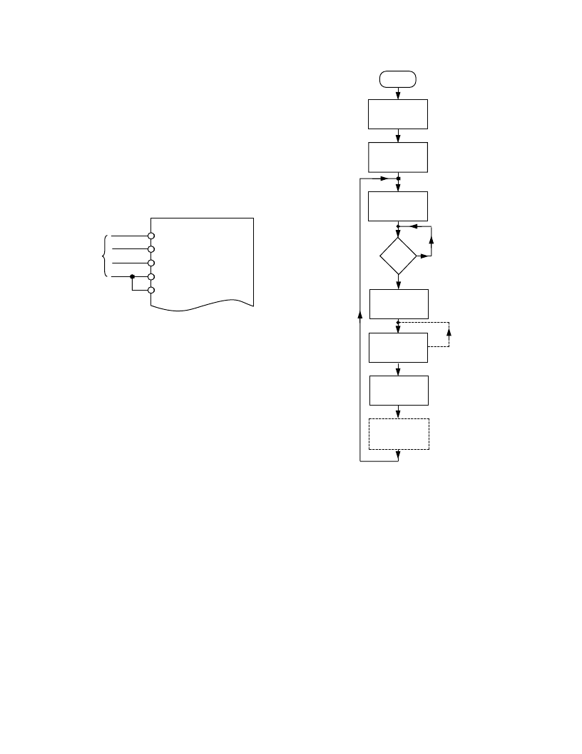
Figure 16. Flowchart for Continuous Read Operations to
the AD7712
The flowchart for Figure 17 is for a single 24-bit write operation
to the AD7712 control or calibration registers. This shows data
being transferred from data memory to the accumulator before
being written to the serial buffer. Some microprocessor systems
will allow data to be written directly to the serial buffer from
data memory. The writing of data to the serial buffer from the
accumulator will generally consist of either two or three write
operations, depending on the size of the serial buffer.
The flowchart also shows the option of the bits being reversed
before being written to the serial buffer. This depends on
whether the first bit transmitted by the microprocessor is the
MSB or the LSB. The AD7712 expects the MSB as the first bit
in the data stream. In cases where the data is being read or
being written in bytes and the data has to be reversed, the bits
will have to be reversed for every byte.
SIMPLIFYING THE EXTERNAL CLOCKING MODE
INTERFACE
In many applications, the user may not require the facility of
writing to the on-chip calibration registers. In this case, the
serial interface to the AD7712 in external clocking mode can be
simplified by connecting the
TFS
line to the A0 input of the
AD7712 (see Figure 15). This means that any write to the de-
vice will load data to the control register (since A0 is low while
TFS
is low) and any read to the device will access data from the
output data register or from the calibration registers (since A0 is
high while
RFS
is low). It should be noted that in this arrange-
ment the user does not have the capability of reading from the
control register.
AD7712
SDATA
SCLK
TFS
A0
FOUR INTER-
FACE LINES
RFS
Figure 15. Simplified Interface with
TFS
Connected to A0
Another method of simplifying the interface is to generate the
TFS
signal from an inverted
RFS
signal. However, generating
the signals the opposite way around (
RFS
from an inverted
TFS
) will cause writing errors.
MICROCOMPUTER/MICROPROCESSOR INTERFACING
The AD7712’s flexible serial interface allows for easy interface
to most microcomputers and microprocessors. Figure 16 shows
a flowchart diagram for a typical programming sequence for
reading data from the AD7712 to a microcomputer while Figure
17 shows a flowchart diagram for writing data to the AD7712.
Figures 18, 19 and 20 show some typical interface circuits.
The flowchart of Figure 16 is for continuous read operations
from the AD7712 output register. In the example shown, the
DRDY
line is continuously polled. Depending on the micropro-
cessor configuration, the
DRDY
line may come to an interrupt
input in which case the
DRDY
will automatically generate an
interrupt without being polled. The reading of the serial buffer
could be anything from one read operation up to three read
operations (where 24 bits of data are read into an 8-bit serial
register). A read operation to the control/calibration registers is
similar, but in this case the status of
DRDY
can be ignored. The
A0 line is brought low when the
RFS
line is brought low when
reading from the control register.
The flowchart also shows the bits being reversed after they have
been read in from the serial port. This depends on whether the
microprocessor expects the MSB of the word first or the LSB of
the word first. The AD7712 outputs the MSB first.
相關(guān)PDF資料 |
PDF描述 |
|---|---|
| AD7712AR | LC2MOS Signal Conditioning ADC |
| AD7712SQ | LC2MOS Signal Conditioning ADC |
| AD7712* | Rail-to-Rail, Very Low Noise Universal Dual Filter Building Block; Package: SSOP; No of Pins: 16; Temperature Range: 0°C to +70°C |
| AD7712 | Signal Conditioning ADC(LC2MOS信號(hào)調(diào)節(jié)A/D轉(zhuǎn)換器) |
| AD7713* | LC2MOS Loop-Powered Signal Conditioning ADC |
相關(guān)代理商/技術(shù)參數(shù) |
參數(shù)描述 |
|---|---|
| AD7712AR | 功能描述:IC ADC SIGNAL COND LC2MOS 24SOIC RoHS:否 類別:集成電路 (IC) >> 數(shù)據(jù)采集 - 模數(shù)轉(zhuǎn)換器 系列:- 標(biāo)準(zhǔn)包裝:1 系列:- 位數(shù):14 采樣率(每秒):83k 數(shù)據(jù)接口:串行,并聯(lián) 轉(zhuǎn)換器數(shù)目:1 功率耗散(最大):95mW 電壓電源:雙 ± 工作溫度:0°C ~ 70°C 安裝類型:通孔 封裝/外殼:28-DIP(0.600",15.24mm) 供應(yīng)商設(shè)備封裝:28-PDIP 包裝:管件 輸入數(shù)目和類型:1 個(gè)單端,雙極 |
| AD7712AR-REEL | 制造商:Analog Devices 功能描述:ADC Single Delta-Sigma 1.028ksps 24-bit Serial 24-Pin SOIC W T/R 制造商:Analog Devices 功能描述:ADC SGL DELTA-SIGMA 1.028KSPS 24BIT SERL 24SOIC W - Tape and Reel |
| AD7712AR-REEL7 | 功能描述:IC ADC 24BIT SGNL CONDTNR 24SOIC RoHS:否 類別:集成電路 (IC) >> 數(shù)據(jù)采集 - 模數(shù)轉(zhuǎn)換器 系列:- 標(biāo)準(zhǔn)包裝:1 系列:- 位數(shù):14 采樣率(每秒):83k 數(shù)據(jù)接口:串行,并聯(lián) 轉(zhuǎn)換器數(shù)目:1 功率耗散(最大):95mW 電壓電源:雙 ± 工作溫度:0°C ~ 70°C 安裝類型:通孔 封裝/外殼:28-DIP(0.600",15.24mm) 供應(yīng)商設(shè)備封裝:28-PDIP 包裝:管件 輸入數(shù)目和類型:1 個(gè)單端,雙極 |
| AD7712ARZ | 功能描述:IC ADC SIGNAL COND LC2MOS 24SOIC RoHS:是 類別:集成電路 (IC) >> 數(shù)據(jù)采集 - 模數(shù)轉(zhuǎn)換器 系列:- 標(biāo)準(zhǔn)包裝:1 系列:microPOWER™ 位數(shù):8 采樣率(每秒):1M 數(shù)據(jù)接口:串行,SPI? 轉(zhuǎn)換器數(shù)目:1 功率耗散(最大):- 電壓電源:模擬和數(shù)字 工作溫度:-40°C ~ 125°C 安裝類型:表面貼裝 封裝/外殼:24-VFQFN 裸露焊盤 供應(yīng)商設(shè)備封裝:24-VQFN 裸露焊盤(4x4) 包裝:Digi-Reel® 輸入數(shù)目和類型:8 個(gè)單端,單極 產(chǎn)品目錄頁(yè)面:892 (CN2011-ZH PDF) 其它名稱:296-25851-6 |
| AD7712ARZ | 制造商:Analog Devices 功能描述:A/D Converter (A-D) IC |
發(fā)布緊急采購(gòu),3分鐘左右您將得到回復(fù)。