- 您現(xiàn)在的位置:買賣IC網(wǎng) > PDF目錄373914 > AD7714AR-3 (ANALOG DEVICES INC) VARISTOR 300V RMS 14MM RADIAL PDF資料下載
參數(shù)資料
| 型號: | AD7714AR-3 |
| 廠商: | ANALOG DEVICES INC |
| 元件分類: | ADC |
| 英文描述: | VARISTOR 300V RMS 14MM RADIAL |
| 中文描述: | 5-CH 24-BIT DELTA-SIGMA ADC, SERIAL ACCESS, PDSO24 |
| 封裝: | WSOIC-24 |
| 文件頁數(shù): | 12/40頁 |
| 文件大小: | 306K |
| 代理商: | AD7714AR-3 |
第1頁第2頁第3頁第4頁第5頁第6頁第7頁第8頁第9頁第10頁第11頁當前第12頁第13頁第14頁第15頁第16頁第17頁第18頁第19頁第20頁第21頁第22頁第23頁第24頁第25頁第26頁第27頁第28頁第29頁第30頁第31頁第32頁第33頁第34頁第35頁第36頁第37頁第38頁第39頁第40頁
AD7714
REV. C
–12–
AD7714-3 OUTPUT NOISE
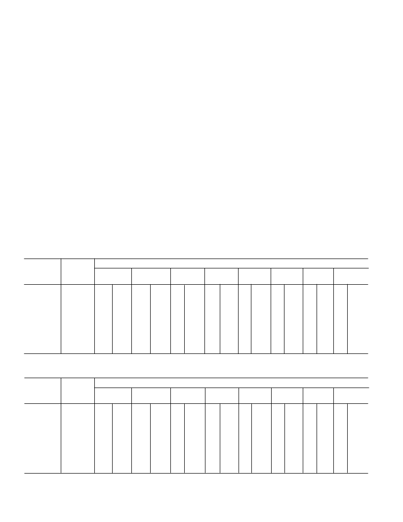
Table IIa shows the output rms noise and effective resolution for some typical notch and –3dB frequencies for the AD7714-3 with
f
CLKIN
= 2.4576MHz while Table IIb gives the information for f
CLK IN
= 1MHz. The numbers given are for the bipolar input
ranges with a V
REF
of +1.25V and BUFFER = 0. These numbers are typical and are generated at an analog input voltage of 0V.
The numbers in brackets in each table are for the effective resolution of the part (rounded to the nearest 0.5LSB). The effective
resolution of the device is defined as the ratio of the output rms noise to the input full scale (i.e., 2
×
V
REF
/GAIN). It should be
noted that it is not calculated using peak-to-peak output noise numbers. Peak-to-peak noise numbers can be up to 6.6 times the rms
numbers while effective resolution numbers based on peak-to-peak noise can be 2.5 bits below the effective resolution based on rms
noise as quoted in the tables.
The output noise from the part comes from two sources. The first is the electrical noise in the semiconductor devices used in the
implementation of the modulator (device noise). Secondly, when the analog input signal is converted into the digital domain, quan-
tization noise is added. The device noise is at a low level and is largely independent of frequency. The quantization noise starts at
an even lower level but rises rapidly with increasing frequency to become the dominant noise source. Consequently, lower filter
notch settings (below 100Hz approximately for f
CLK IN
= 2.4576MHz and below 40Hz approximately for f
CLK IN
= 1MHz) tend to
be device noise dominated while higher notch settings are dominated by quantization noise. Changing the filter notch and cutoff
frequency in the quantization noise dominated region results in a more dramatic improvement in noise performance than it does in
the device-noise dominated region as shown in Table II. Furthermore, quantization noise is added after the PGA, so effective reso-
lution is largely independent of gain for the higher filter notch frequencies. Meanwhile, device noise is added in the PGA and, there-
fore, effective resolution suffers a little at high gains for lower notch frequencies. Additionally, in the device-noise dominated region,
the output noise (in
μ
V) is largely independent of reference voltage while in the quantization-noise dominated region, the noise is
proportional to the value of the reference. It is possible to do post-filtering on the device to improve the output data ratefor a given
–3dB frequency and also to further reduce the output noise.
At the lower filter notch settings (below 60Hz for f
CLK IN
= 2.4576MHz and below 25Hz for f
CLK IN
= 1MHz), the no missing
codes performance of the device is at the 24-bit level. At the higher settings, more codes will be missed until at 1kHz notch setting
for f
CLKIN
= 2.4576MHz (400Hz for f
CLK IN
= 1MHz), no missing codes performance is only guaranteed to the 12-bit level.
Filter First
Notch & O/P
Data Rate
Typical Output RMS Noise in
m
V (Effective Resolution in Bits)
Gain of
Gain of
Gain of
2
4
8
–3dB
Frequency
Gain of
Gain of
16
Gain of
32
Gain of
64
Gain of
128
1
2Hz
4Hz
10Hz
25Hz
30Hz
50Hz
60Hz
100Hz
200Hz
400 Hz
0.52Hz
1.05Hz
2.62Hz
6.55Hz
7.86Hz
13.1Hz
15.72Hz
26.2Hz
52.4Hz
104.8Hz
0.86
1.26
1.68
3.82
4.88
11
14.7
61
275
1435 (11)
(21.5)
(21)
(20.5)
(19.5)
(19)
(18)
(17.5)
(15.5)
(13)
0.58
0.74
1.33
2.0
2.1
4.8
7.5
30
130
720
(21)
(20.5)
(20)
(19.5)
(19)
(18)
(17.5)
(15.5)
(13)
(11)
0.32 (21)
0.44 (20.5)
0.73 (20)
1.2
(19)
1.3
(19)
2.4
(18)
3.8
(17.5)
12
(15.5)
65
(13)
362 (11)
0.21 (20.5) 0.2
0.35 (20)
0.5
(19)
0.88 (18.5) 0.66 (18)
0.93 (18.5) 0.82 (17.5) 0.69 (17)
1.4
(18)
1.4
2.6
(17)
1.5
6.1
(15.5) 2.9
33
(13)
17
175 (11)
110 (10.5) 51
(19.5) 0.2
(19)
(18.5) 0.2
(18)
(17.5) 0.2
(17)
(16.5)
(16)
0.3
0.49 (18.5) 0.49 (17.5) 0.48 (16.5) 0.47 (15.5)
0.57 (17)
0.3
0.3
0.3
0.55 (16)
0.68 (16)
0.55 (15)
0.66 (15)
(17)
(16.5) 0.95 (16.5) 0.88 (15)
(15.5) 2.4
(15)
(13)
11
(13)
(10.5) 31
0.73 (16.5) 0.71 (15.5) 0.7
(15)
(14.5)
(13.5)
(12.5)
(10.5)
0.9
1.8
6.3
(14.5) 1.8
(12.5) 3
(10.5) 12
Table IIa. AD7714-3 Output Noise/Resolution vs. Gain and First Notch for f
CLK IN
= 2.4576MHz, BUFFER = 0
Filter First
Notch & O/P
Data Rate
Typical Output RMS Noise in
m
V (Effective Resolution in Bits)
Gain of
Gain of
Gain of
2
4
8
–3dB
Frequency
Gain of
Gain of
16
Gain of
32
Gain of
64
Gain of
128
1
5Hz
10Hz
25Hz
30Hz
50Hz
60Hz
100Hz
250Hz
500Hz
1kHz
1.31Hz
2.62Hz
6.55Hz
7.86Hz
13.1Hz
15.72Hz
26.2Hz
65.5Hz
131Hz
262Hz
1.07
1.69
3.03
3.55
4.72
5.12
9.68
44
304
1410 (11)
(21)
(20.5)
(19.5)
(19.5)
(19)
(19)
(18)
(16)
(13)
0.68
1.1
1.7
2.1
2.3
3.1
5.6
31
129
715
(21)
(20)
(19.5)
(19)
(19)
(18.5)
(18)
(15.5)
(13)
(11)
0.29 (21)
0.56 (20)
0.89 (19.5)
1.1
(19)
1.5
(18.5)
1.6
(18)
2.4
(18)
15
(15.5)
76
(13)
350 (11)
0.24 (20)
0.35 (19.5) 0.33 (19)
0.55 (19)
0.61 (18.5) 0.58 (18)
0.84 (18.5) 0.7
0.98 (18)
1.3
(18)
5.8
(15.5) 3.7
33
(13)
177 (11)
0.22 (19.5) 0.22 (18.5) 0.22 (17.5) 0.22 (16.5)
0.33 (18)
0.49 (18.5) 0.46 (17.5) 0.46 (16.5) 0.45 (15.5)
0.57 (17)
(18)
0.68 (17)
0.9
(17.5) 0.7
(17)
1.1
(17)
0.95 (16.5) 0.88 (15.5) 0.9
(15.5) 2.4
(15)
20
(13)
11
(13)
101 (10.5) 51
(10.5) 31
0.33 (17)
0.33 (16)
0.55 (16)
0.67 (16)
0.69 (16)
0.55 (15)
0.66 (15)
0.68 (15)
(14.5)
(13.5)
(12.5)
(10.5)
1.8
6.3
(14.5) 1.8
(12.5) 3
(10.5) 12
Table IIb. AD7714-3 Output Noise/Resolution vs. Gain and First Notch for f
CLK IN
= 1MHz, BUFFER = 0
相關(guān)PDF資料 |
PDF描述 |
|---|---|
| AD7714AR-5 | Metal Oxide Varistor (MOV); Voltage Rating AC, Vrms:680Vrms; Voltage Rating DC, Vdc:895VDC; Peak Surge Current (8/20uS), Itm:4500A; Clamping Voltage 8/20us Max :1815V; Capacitance, Cd:140pF; Package/Case:14mm Disc |
| AD7714 | Signal Conditioning ADC(信號調(diào)節(jié)A/D轉(zhuǎn)換器) |
| AD7715ARU-3 | 3 V/5 V, 450 uA 16-Bit, Sigma-Delta ADC |
| AD7715ARU-5 | AB 4C 4#12 PIN RECP |
| AD7715AN-3 | 3 V/5 V, 450 uA 16-Bit, Sigma-Delta ADC |
相關(guān)代理商/技術(shù)參數(shù) |
參數(shù)描述 |
|---|---|
| AD7714AR-3REEL | 功能描述:IC ADC 24BIT SIGMA-DELTA 24-SOIC RoHS:否 類別:集成電路 (IC) >> 數(shù)據(jù)采集 - 模數(shù)轉(zhuǎn)換器 系列:- 標準包裝:1,000 系列:- 位數(shù):12 采樣率(每秒):300k 數(shù)據(jù)接口:并聯(lián) 轉(zhuǎn)換器數(shù)目:1 功率耗散(最大):75mW 電壓電源:單電源 工作溫度:0°C ~ 70°C 安裝類型:表面貼裝 封裝/外殼:24-SOIC(0.295",7.50mm 寬) 供應商設備封裝:24-SOIC 包裝:帶卷 (TR) 輸入數(shù)目和類型:1 個單端,單極;1 個單端,雙極 |
| AD7714AR-5 | 功能描述:IC ADC SIGNAL COND 5V 24-SOIC RoHS:否 類別:集成電路 (IC) >> 數(shù)據(jù)采集 - 模數(shù)轉(zhuǎn)換器 系列:- 標準包裝:1,000 系列:- 位數(shù):12 采樣率(每秒):300k 數(shù)據(jù)接口:并聯(lián) 轉(zhuǎn)換器數(shù)目:1 功率耗散(最大):75mW 電壓電源:單電源 工作溫度:0°C ~ 70°C 安裝類型:表面貼裝 封裝/外殼:24-SOIC(0.295",7.50mm 寬) 供應商設備封裝:24-SOIC 包裝:帶卷 (TR) 輸入數(shù)目和類型:1 個單端,單極;1 個單端,雙極 |
| AD7714AR-5REEL | 功能描述:IC ADC 24BIT SIGMA-DELTA 24-SOIC RoHS:否 類別:集成電路 (IC) >> 數(shù)據(jù)采集 - 模數(shù)轉(zhuǎn)換器 系列:- 標準包裝:1,000 系列:- 位數(shù):12 采樣率(每秒):300k 數(shù)據(jù)接口:并聯(lián) 轉(zhuǎn)換器數(shù)目:1 功率耗散(最大):75mW 電壓電源:單電源 工作溫度:0°C ~ 70°C 安裝類型:表面貼裝 封裝/外殼:24-SOIC(0.295",7.50mm 寬) 供應商設備封裝:24-SOIC 包裝:帶卷 (TR) 輸入數(shù)目和類型:1 個單端,單極;1 個單端,雙極 |
| AD7714AR-5Z | 制造商:Analog Devices 功能描述:ADC 24BIT 5CH PGA 24SOIC 制造商:Analog Devices 功能描述:ADC, 24BIT, 5CH PGA, 24SOIC; Resolution (Bits):24bit; Sampling Rate:1kSPS; Supply Voltage Type:Single; Supply Voltage Min:4.75V; Supply Voltage Max:5.25V; Supply Current:1.1mA; Digital IC Case Style:SOIC; No. of Pins:24; Input ;RoHS Compliant: Yes |
| AD7714ARS-3 | 功能描述:IC ADC 24BIT SIGMA-DELTA 28SSOP RoHS:否 類別:集成電路 (IC) >> 數(shù)據(jù)采集 - 模數(shù)轉(zhuǎn)換器 系列:- 標準包裝:1,000 系列:- 位數(shù):12 采樣率(每秒):300k 數(shù)據(jù)接口:并聯(lián) 轉(zhuǎn)換器數(shù)目:1 功率耗散(最大):75mW 電壓電源:單電源 工作溫度:0°C ~ 70°C 安裝類型:表面貼裝 封裝/外殼:24-SOIC(0.295",7.50mm 寬) 供應商設備封裝:24-SOIC 包裝:帶卷 (TR) 輸入數(shù)目和類型:1 個單端,單極;1 個單端,雙極 |
發(fā)布緊急采購,3分鐘左右您將得到回復。