- 您現在的位置:買賣IC網 > PDF目錄373914 > AD7714YRU (ANALOG DEVICES INC) 3 V/5 V, CMOS, 500 uA Signal Conditioning ADC PDF資料下載
參數資料
| 型號: | AD7714YRU |
| 廠商: | ANALOG DEVICES INC |
| 元件分類: | ADC |
| 英文描述: | 3 V/5 V, CMOS, 500 uA Signal Conditioning ADC |
| 中文描述: | 5-CH 24-BIT DELTA-SIGMA ADC, SERIAL ACCESS, PDSO24 |
| 封裝: | TSSOP-24 |
| 文件頁數: | 17/40頁 |
| 文件大小: | 306K |
| 代理商: | AD7714YRU |
第1頁第2頁第3頁第4頁第5頁第6頁第7頁第8頁第9頁第10頁第11頁第12頁第13頁第14頁第15頁第16頁當前第17頁第18頁第19頁第20頁第21頁第22頁第23頁第24頁第25頁第26頁第27頁第28頁第29頁第30頁第31頁第32頁第33頁第34頁第35頁第36頁第37頁第38頁第39頁第40頁
2
AD7714
REV. C
–17–
Filter Registers. Power On/Reset Status: Filter High Register: 01Hex. Filter Low Register: 40Hex.
There are two 8-bit Filter Registers on the AD7714 from which data can either be read or to which data can be written. Tables IX
and X outline the bit designations for the Filter Registers.
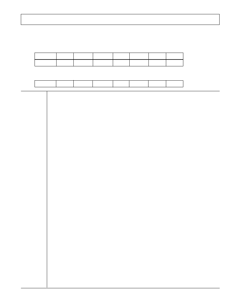
Table IX. Filter High Register (RS2–RS0 = 0, 1, 0)
B
/U
WL
BST
ZERO
FS11
FS10
FS9
FS8
A Versions
B
/U
WL
BST
CLKDIS
FS11
FS10
FS9
FS8
Y Versions
Table X. Filter Low Register (RS2–RS0 = 0, 1, 1)
FS7
FS6
FS5
FS4
FS3
FS2
FS1
FS0
All Versions
B
/U
Bipolar/Unipolar Operation. A 0 in this bit selects Bipolar Operation. This is the default (Power-On or RESET)
status of this bit. A 1 in this bit selects unipolar operation.
Word Length. A 0 in this bit selects 16-bit word length when reading from the data register (i.e.,
DRDY
returns
high after 16 serial clock cycles in the read operation). This is the default (Power-On or RESET) status of this
bit. A 1 in this bit selects 24-bit word length.
Current Boost. A 0 in this bit reduces the current taken by the analog front end. When the part is operated with
f
CLK IN
= 1MHz or at gains of 1 to 4 with f
CLK IN
= 2.4576MHz, this bit should be 0 to reduce the current
drawn from AV
DD
, although the device will operate just as well with this bit at a 1. When the AD7714 is oper-
ated at gains of 8 to 128 with f
CLK IN
= 2.4576MHz, this bit
must be
1 to ensure correct operation of the
device. The Power-On or RESET status of this bit is 0.
To ensure correct operation of the A Versions of the part, a 0
must be
written to this bit.
Master Clock Disable Bit. A Logic 1 in this bit disables the master clock from appearing at the MCLKOUT
pin. When disabled, the MCLKOUT pin is forced low. This feature allows the user the flexibility of using the
MCLKOUT as a clock source for other devices in the system or for turning off the MCLKOUT as a power
saving feature. When using an external master clock or the MCLKIN pin, the AD7714 continues to have inter-
nal clocks and will convert normally with its CLKDIS bit active. When using a crystal oscillator or ceramic
resonator across the MCLK IN or MCLKOUT pins, the AD7714 clock is stopped and no conversions take
place when the CLKDIS bit is active.
Filter Selection. The on-chip digital filter provides a Sinc
3
(or (Sinx/x)
3
) filter response. The 12 bits of data
programmed into these bits determine the filter cut-off frequency, the position of the first notch of the filter and
the data rate for the part. In association with the gain selection, it also determines the output noise (and hence
the effective resolution) of the device.
The first notch of the filter occurs at a frequency determined by the relationship:
filter first notch frequency =(f
CLKIN
/128)/code
where
code
is the decimal equivalent of the code in bits FS0 to FS11 and is in the range 19 to 4,000. With the
nominal f
CLK IN
of 2.4576MHz, this results in a first notch frequency range from 4.8Hz to 1.01kHz. To
ensure correct operation of the AD7714, the value of the code loaded to these bits must be within this range.
Failure to do this will result in unspecified operation of the device.
Changing the filter notch frequency, as well as the selected gain, impacts resolution. Tables I through IV show
the effect of the filter notch frequency and gain on the effective resolution of the AD7714. The output data rate
(or effective conversion time) for the device is equal to the frequency selected for the first notch of the filter. For
example, if the first notch of the filter is selected at 50Hz then a new word is available at a 50 Hz rate or every
20ms. If the first notch is at 1kHz, a new word is available every 1ms.
The settling time of the filter to a full-scale step input change is worst case 4
×
1/(output data rate). For
example, with the first filter notch at 50Hz, the settling time of the filter to a full-scale step input change is
80ms max. This settling time can be reduced to 3
×
1/(output data rate) by synchronizing the step input
change to a reset of the digital filter. In other words, if the step input takes place with the
SYNC
input low or
the FSYNC bit high, the settling time will be 3
×
1/(output data rate) from when
SYNC
returns high or
FSYNC returns low. If a change of channel takes place, the settling time is 3
×
1/(output data rate) regardless of
the
SYNC
or FSYNC status as the part issues an internal
SYNC
command when requested to change channels.
The –3 dB frequency is determined by the programmed first notch frequency according to the relationship:
filter –3 dB frequency = 0.262
×
filter first notch frequency.
WL
BST
ZERO
CLKDIS
FS11–FS0
相關PDF資料 |
PDF描述 |
|---|---|
| AD7714* | 3 V/5 V. CMOS. 500 uA Signal Conditioning ADC |
| AD7714ARS-3 | 3 V/5 V, CMOS, 500 uA Signal Conditioning ADC |
| AD7714ARS-5 | 3 V/5 V, CMOS, 500 uA Signal Conditioning ADC |
| AD7714ACHIPS-3 | 3 V/5 V, CMOS, 500 uA Signal Conditioning ADC |
| AD7714ACHIPS-5 | 3 V/5 V, CMOS, 500 uA Signal Conditioning ADC |
相關代理商/技術參數 |
參數描述 |
|---|---|
| AD7714YRU-REEL | 制造商:Analog Devices 功能描述:ADC Single Delta-Sigma 1ksps 24-bit Serial 24-Pin TSSOP T/R 制造商:Analog Devices 功能描述:ADC SGL DELTA-SIGMA 1KSPS 24BIT SERL 24TSSOP - Tape and Reel |
| AD7714YRU-REEL7 | 功能描述:IC ADC 24BIT SIGMA-DELTA 24TSSOP RoHS:否 類別:集成電路 (IC) >> 數據采集 - 模數轉換器 系列:- 標準包裝:1,000 系列:- 位數:12 采樣率(每秒):300k 數據接口:并聯 轉換器數目:1 功率耗散(最大):75mW 電壓電源:單電源 工作溫度:0°C ~ 70°C 安裝類型:表面貼裝 封裝/外殼:24-SOIC(0.295",7.50mm 寬) 供應商設備封裝:24-SOIC 包裝:帶卷 (TR) 輸入數目和類型:1 個單端,單極;1 個單端,雙極 |
| AD7714YRUZ | 功能描述:IC ADC SIGNAL COND 3/5V 24-TSSOP RoHS:是 類別:集成電路 (IC) >> 數據采集 - 模數轉換器 系列:- 標準包裝:1 系列:microPOWER™ 位數:8 采樣率(每秒):1M 數據接口:串行,SPI? 轉換器數目:1 功率耗散(最大):- 電壓電源:模擬和數字 工作溫度:-40°C ~ 125°C 安裝類型:表面貼裝 封裝/外殼:24-VFQFN 裸露焊盤 供應商設備封裝:24-VQFN 裸露焊盤(4x4) 包裝:Digi-Reel® 輸入數目和類型:8 個單端,單極 產品目錄頁面:892 (CN2011-ZH PDF) 其它名稱:296-25851-6 |
| AD7714YRUZ | 制造商:Analog Devices 功能描述:A/D Converter (A-D) IC |
| AD7714YRUZ-REEL | 功能描述:IC ADC 24BIT SIGMA-DELTA 24TSSOP RoHS:是 類別:集成電路 (IC) >> 數據采集 - 模數轉換器 系列:- 標準包裝:1,000 系列:- 位數:12 采樣率(每秒):300k 數據接口:并聯 轉換器數目:1 功率耗散(最大):75mW 電壓電源:單電源 工作溫度:0°C ~ 70°C 安裝類型:表面貼裝 封裝/外殼:24-SOIC(0.295",7.50mm 寬) 供應商設備封裝:24-SOIC 包裝:帶卷 (TR) 輸入數目和類型:1 個單端,單極;1 個單端,雙極 |
發布緊急采購,3分鐘左右您將得到回復。