- 您現(xiàn)在的位置:買賣IC網(wǎng) > PDF目錄373915 > AD7740YRT (ANALOG DEVICES INC) 3 V/5 V Low Power, Synchronous Voltage-to-Frequency Converter PDF資料下載
參數(shù)資料
| 型號(hào): | AD7740YRT |
| 廠商: | ANALOG DEVICES INC |
| 元件分類: | 模擬專用變換器 |
| 英文描述: | 3 V/5 V Low Power, Synchronous Voltage-to-Frequency Converter |
| 中文描述: | VOLTAGE-FREQUENCY CONVERTER, 1 MHz, PDSO8 |
| 封裝: | SOT-23, 8 PIN |
| 文件頁(yè)數(shù): | 2/11頁(yè) |
| 文件大小: | 144K |
| 代理商: | AD7740YRT |
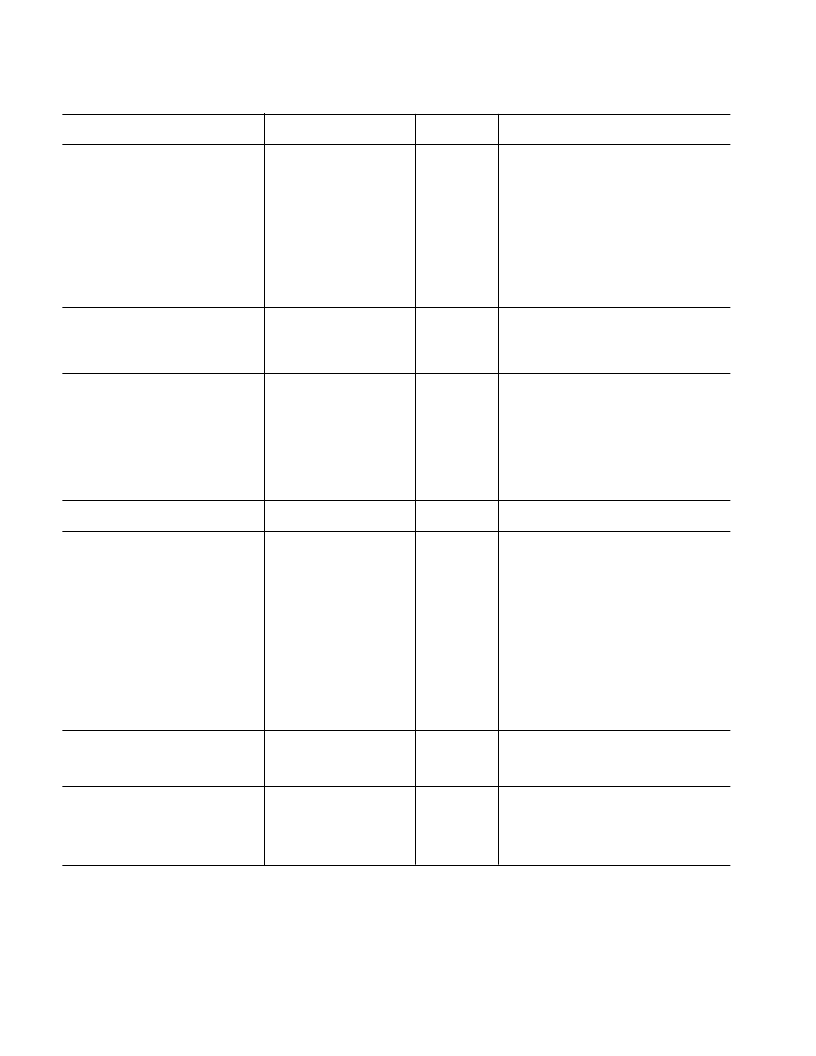
AD7740 SPECIFICATIONS
K, Y Versions
1
Min
Typ
Parameter
2
Max
Unit
Test Conditions/Comments
DC PERFORMANCE
Integral Nonlinearity
CLKIN = 32 kHz
3
CLKIN = 1 MHz
CLKIN = 32 kHz
3
CLKIN = 1 MHz
Offset Error
±
0.012
±
0.012
±
0.018
±
0.018
±
35
±
35
±
0.7
% of Span
4
% of Span
% of Span
% of Span
mV
mV
% of Span
μ
V/
°
C
ppm of Span/
°
C
dB
dB
Unbuffered Mode, External Clock at CLKIN
Unbuffered Mode, Crystal at CLKIN
Buffered Mode, External Clock at CLKIN
Buffered Mode, Crystal at CLKIN
Unbuffered Mode, VIN = 0 V
Buffered Mode, VIN = 0.1 V
±
7
±
7
±
0.1
±
20
±
4
–55
–65
Gain Error
Offset Error Drift
3
Gain Error Drift
3
Power Supply Rejection Ratio
3
VDD =
±
5% (5 V)
VDD =
±
10% (3.3 V)
ANALOG INPUT, VIN
Nominal Input Span
0 – V
REF
V
V
μ
A
nA
±
150 mV Overrange Available
Buffered Mode
Unbuffered Mode, VIN = 5.4 V, REFIN = 5.25 V
Buffered Mode, VIN = 0.1 V, REFIN = 2.5 V
0.1
VDD – 0.2
10
100
Input Current
8
5
REFERENCE VOLTAGE
REFIN
5
Nominal Input Voltage
REFOUT
Output Voltage
Output Impedance
3
Reference Drift
3
Line Rejection
3
Line Rejection
3
Reference Noise (0.1 Hz to 10 Hz)
3
FOUT OUTPUT
Nominal Frequency Span
LOGIC INPUTS (CLKIN, BUF)
3
CLKIN
Input frequency
Input High Voltage, V
IH
Input High Voltage, V
IH
Input Low Voltage, V
IL
Input Low Voltage, V
IL
Input Current
Pin Capacitance
BUF
Input High Voltage, V
IH
Input High Voltage, V
IH
Input Low Voltage, V
IL
Input Low Voltage, V
IL
Input Current
Pin Capacitance
LOGIC OUTPUTS (FOUT, CLKOUT)
3
Output High Voltage, V
OH
Output High Voltage, V
OH
Output Low Voltage, V
OL
2.5
VDD
V
2.3
2.5
1
±
50
–75
–60
100
2.7
V
k
ppm/
°
C
dB
dB
μ
V p–p
See Pin Function Description
VDD =
±
5% (5 V)
VDD =
±
10% (3.3 V)
0.1 f
CLKIN
to 0.9 f
CLKIN
Hz
VIN = 0 V to V
REF
. See Figure 2
32
3.5
2.5
1000
kHz
V
V
V
V
μ
A
pF
For Specified Performance
VDD = 5 V
±
5%
VDD = 3.3 V
±
10%
VDD = 5 V
±
5%
VDD = 3.3 V
±
10%
VIN = 0 V to V
DD
0.8
0.4
±
2
10
3
2.4
2.1
V
V
V
V
nA
pF
VDD = 5 V
±
5%
VDD = 3.3 V
±
10%
VDD = 5 V
±
5%
VDD = 3.3 V
±
10%
0.8
0.4
±
100
10
3
4.0
2.1
V
V
V
Output Sourcing 200
μ
A
6
. VDD = 5 V
±
5%
Output Sourcing 200
μ
A
6
. VDD = 3.3 V
±
10%
Output Sinking 1.6 mA
6
0.1
0.4
POWER REQUIREMENTS
V
DD7
I
DD
(Normal Mode)
8
I
DD
(Normal Mode)
8
I
DD
(Power-Down)
Power-Up Time
NOTES
1
Temperature range: K Version, 0
°
C to +85
°
C; Y Version, –40
°
C to +105
°
C; typical specifications are at 25
°
C.
2
See Terminology.
3
Guaranteed by design and characterization, not production tested.
4
Span = Max output frequency–Min output frequency.
5
Because this pin is bidirectional, any external reference must be capable of sinking/sourcing 400
μ
A in order to overdrive the internal reference.
6
These logic levels apply to CLKOUT only when it is loaded with one CMOS load.
7
Operation at VDD = 2.7 V is also possible with degraded specifications.
8
Outputs unloaded. I
increases by C
L
×
V
OUT
×
f
FOUT
when FOUT is loaded. If using a crystal/resonator as the clock source, I
DD
will vary depending on the crystal/resonator
type (see Clock Generation section).
Specifications subject to change without notice.
3.0
5.25
1.25
1.5
100
V
mA
mA
μ
A
μ
s
0.9
1.1
30
30
V
IH
= VDD, V
IL
= GND. Unbuffered Mode
V
IH
= VDD, V
IL
= GND. Buffered Mode
Exiting Power-Down (Ext. Clock at CLKIN)
REV. 0
–2–
(VDD = 3.0 V to 3.6 V, 4.75 V to 5.25 V, GND = 0 V, REFIN = 2.5 V; CLKIN = 1 MHz; All
specifications T
MIN
to T
MAX
unless otherwise noted.)
相關(guān)PDF資料 |
PDF描述 |
|---|---|
| AD7740 | 3 V/5 V Low Power, Synchronous Voltage-to-Frequency Converter |
| AD7740YRM | 3 V/5 V Low Power, Synchronous Voltage-to-Frequency Converter |
| AD7741YR | Single and Multichannel, Synchronous Voltage-to-Frequency Converters |
| AD7742YR | Single and Multichannel, Synchronous Voltage-to-Frequency Converters |
| AD7741BN | Single and Multichannel, Synchronous Voltage-to-Frequency Converters |
相關(guān)代理商/技術(shù)參數(shù) |
參數(shù)描述 |
|---|---|
| AD7740YRT-REEL | 制造商:Analog Devices 功能描述: |
| AD7740YRT-REEL7 | 制造商:Rochester Electronics LLC 功能描述:LOW COST SMALL SYNCHRONOUS VFC ADC. I.C. - Tape and Reel 制造商:Analog Devices 功能描述: |
| AD7740YRTZ-REEL7 | 功能描述:IC CONVERTER VOLT-FREQ SOT23-8 RoHS:是 類別:集成電路 (IC) >> PMIC - V/F 和 F/V 轉(zhuǎn)換器 系列:- 標(biāo)準(zhǔn)包裝:1 系列:- 類型:頻率至電壓 頻率 - 最大:10kHz 全量程:- 線性:±0.3% 安裝類型:表面貼裝 封裝/外殼:8-SOIC(0.154",3.90mm 寬) 供應(yīng)商設(shè)備封裝:8-SOIC 包裝:Digi-Reel® 其它名稱:LM2917MX-8/NOPBDKR |
| AD7741 | 制造商:AD 制造商全稱:Analog Devices 功能描述:Single and Multichannel, Synchronous Voltage-to-Frequency Converters |
| AD7741BN | 制造商:Analog Devices 功能描述:VFC Sync 1.35MHz 8-Pin PDIP Tube 制造商:Rochester Electronics LLC 功能描述:SINGLE + MULTI-CHANNEL VFC I.C. - Bulk 制造商:Analog Devices 功能描述:IC VOLTAGE-FREQ CONVERTER |
發(fā)布緊急采購(gòu),3分鐘左右您將得到回復(fù)。