- 您現在的位置:買賣IC網 > PDF目錄373915 > AD7742BN (ANALOG DEVICES INC) Single and Multichannel, Synchronous Voltage-to-Frequency Converters PDF資料下載
參數資料
| 型號: | AD7742BN |
| 廠商: | ANALOG DEVICES INC |
| 元件分類: | 模擬專用變換器 |
| 英文描述: | Single and Multichannel, Synchronous Voltage-to-Frequency Converters |
| 中文描述: | VOLTAGE-FREQUENCY CONVERTER, 6.144 MHz, PDIP16 |
| 封裝: | PLASTIC, DIP-16 |
| 文件頁數: | 6/12頁 |
| 文件大小: | 131K |
| 代理商: | AD7742BN |
REV. 0
AD7741/AD7742
–6–
AD7742 PIN FUNCTION DESCRIPTION
Pin No.
Mnemonic
Function
1
2
f
OUT
V
DD
Frequency Output. This pin provides the output of the synchronous VFC.
Power Supply Input. These parts can be operated from +4.75 V to +5.25 V and the supply should be
adequately decoupled to GND.
Ground reference point for all circuitry on the part.
Address Inputs used to select the input channel configuration.
External Clock Output. When the master clock for the device is a crystal, the crystal is connected be-
tween CLKIN and CLKOUT. When an external clock is applied to CLKIN, the CLKOUT pin
provides an inverted clock signal. This clock should be buffered if it is to be used as a clock source
elsewhere in the system.
External Clock Input. The master clock for the device can be provided in the form of a crystal or an
external clock. A crystal may be tied across the CLKIN and CLKOUT pins. Alternatively, the CLKIN
pin may be driven by a CMOS-compatible clock and CLKOUT left unconnected. The frequency of the
master clock may be as high as 6 MHz.
Control input which determines whether the device operates with differential bipolar analog input
signals or differential unipolar analog input signals.
2.5 V Voltage Reference Output. This can be tied directly to REFIN. It may also be used as a reference
to other parts of the system provided it is buffered first.
This is the Reference Input to the core of the VFC and defines the span of the VFC. A 2.5 V reference
is required at this pin. This may be provided by connecting it directly to REFOUT or by using a preci-
sion external reference (e.g., REF192).
Buffered Analog Input Channel 1. This is either a pseudo-differential input with respect to V
IN
4 or it is
the positive input of a truly-differential input pair with respect to V
IN
2.
Buffered Analog Input Channel 2. This is either a pseudo-differential input with respect to V
IN
4 or it is
the negative input of a truly-differential input pair with respect to V
IN
1.
Buffered Analog Input Channel 3. This is the positive input of a truly-differential input pair with re-
spect to V
IN
4.
Buffered Analog Input Channel 4. This is either the common for pseudo-differential input with respect
to V
IN
1 or V
IN
2 or it is the negative input of a truly-differential input pair with respect to V
IN
3.
Gain Select input that controls whether the gain on the analog front-end is X1 or X2.
Active Low Power-Down pin. When this input is low, the part enters power-down mode where it typi-
cally consumes 25
μ
A of current.
3
4–5
6
GND
A1, A0
CLKOUT
7
CLKIN
8
UNI/
BIP
9
REFOUT
10
REFIN
11
V
IN
1
12
V
IN
2
13
V
IN
3
14
V
IN
4
15
16
GAIN
PD
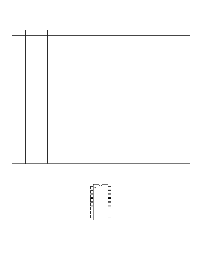
PIN CONFIGURATION
TOP VIEW
(Not to Scale)
16
15
14
13
12
11
10
9
1
2
3
4
5
6
7
8
f
OUT
PD
AD7742
V
DD
GAIN
GND
V
IN
4
A1
V
IN
3
A0
V
IN
2
CLKOUT
V
IN
1
CLKIN
REFIN
UNI/
BIP
REFOUT
相關PDF資料 |
PDF描述 |
|---|---|
| AD7742BR | Single and Multichannel, Synchronous Voltage-to-Frequency Converters |
| AD774BJR | Complete 12-Bit A/D Converters |
| AD774BAR | Complete 12-Bit A/D Converters |
| AD774BBR | Complete 12-Bit A/D Converters |
| AD774BAD | Complete 12-Bit A/D Converters |
相關代理商/技術參數 |
參數描述 |
|---|---|
| AD7742BNZ | 制造商:Analog Devices 功能描述:VFC Sync 2.75MHz 16-Pin PDIP |
| AD7742BR | 制造商:AD 制造商全稱:Analog Devices 功能描述:Single and Multichannel, Synchronous Voltage-to-Frequency Converters |
| AD7742BR-REEL | 制造商:Analog Devices 功能描述: |
| AD7742YR | 制造商:AD 制造商全稱:Analog Devices 功能描述:Single and Multichannel, Synchronous Voltage-to-Frequency Converters |
| AD7742YR-REEL | 制造商:Analog Devices 功能描述: |
發布緊急采購,3分鐘左右您將得到回復。