- 您現(xiàn)在的位置:買賣IC網(wǎng) > PDF目錄373916 > AD774BTD (ANALOG DEVICES INC) Complete 12-Bit A/D Converters PDF資料下載
參數(shù)資料
| 型號: | AD774BTD |
| 廠商: | ANALOG DEVICES INC |
| 元件分類: | ADC |
| 英文描述: | Complete 12-Bit A/D Converters |
| 中文描述: | 1-CH 12-BIT SUCCESSIVE APPROXIMATION ADC, PARALLEL ACCESS, CDIP28 |
| 封裝: | HERMETIC SEALED, CERAMIC, DIP-28 |
| 文件頁數(shù): | 9/12頁 |
| 文件大小: | 247K |
| 代理商: | AD774BTD |
REV. C
–9–
TO
OUTPUT
BUFFERS
CE
CS
R/
C
A
0
12/
8
NYBBLE A
ENABLE
NYBBLE B
ENABLE
NYBBLE C
ENABLE
NYBBLE = 0
ENABLE
STATUS
CLK EN
HIGH IF CONVERSION
IN PROGRESS
SAR
RESET
EOC 12
EOC 8
START CONVERT
S
R
Q
QB
READ
VALUE OF A
0
AT LAST CONVERT COMMAND
D
EN
D
EN
Q
R
S
Q
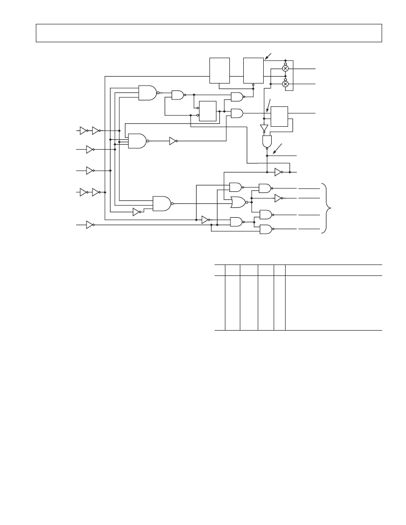
Figure 9. Equivalent Internal Logic Circuitry
CONTROL LOGIC
The AD674B and AD774B contain on-chip logic to provide
conversion initiation and data read operations from signals
commonly available in microprocessor systems; this internal
logic circuitry is shown in Figure 9.
The control signals CE,
CS
, and R/
C
control the operation of
the converter. The state of R/
C
when CE and
CS
are both
asserted determines whether a data read (R/
C
= 1) or a convert
(R/
C
= 0) is in progress. The register control inputs, A
0
and
12/
8
, control conversion length and data format. If a conversion
is started with A
0
low, a full 12-bit conversion cycle is initiated.
If A
0
is high during a convert start, a shorter 8-bit conversion
cycle results. During data read operations, A
0
determines
whether the three-state buffers containing the 8 MSBs of the
conversion result (A
0
= 0) or the 4 LSBs (A
0
= 1) are enabled.
The 12/
8
pin determines whether the output data is to be orga-
nized as two 8-bit words (12/
8
tied to DIGITAL COMMON)
or a single 12-bit word (12/
8
tied to V
LOGIC
). In the 8-bit mode,
the byte addressed when A
0
is high contains the 4 LSBs from
the conversion followed by four trailing zeroes. This organiza-
tion allows the data lines to be overlapped for direct interface to
8-bit buses without the need for external three-state buffers.
An output signal, STS, indicates the status of the converter.
STS goes high at the beginning of a conversion and returns low
when the conversion cycle is complete.
Table I. Truth Table
CE
CS
R/
C
12/
8
A
0
Operation
0
X
1
1
1
1
1
X
1
0
0
0
0
0
X
X
0
0
1
1
1
X
X
X
X
1
0
0
X
X
0
1
X
0
1
None
None
Initiate 12-Bit Conversion
Initiate 8-Bit Conversion
Enable 12-Bit Parallel Output
Enable 8 Most Significant Bits
Enable 4 LSBs + 4 Trailing Zeroes
The ADC may be operated in one of two modes, the full-control
mode and the standalone mode. The full-control mode uses all
the control signals and is useful in systems that address decode
multiple devices on a single data bus. The standalone mode is
useful in systems with dedicated input ports available. In gen-
eral, the standalone mode is capable of issuing start-convert
commands on a more precise basis and therefore produces
higher accuracy results. The following sections describe these
two modes in more detail.
FULL-CONTROL MODE
Chip Enable (CE), Chip Select (
CS
), and Read/Convert (R/
C
)
are used to control Convert or Read modes of operation. Either
CE or
CS
may be used to initiate a conversion. The state of R/
C
when CE and
CS
are both asserted determines whether a data
Read (R/
C
= 1) or a Convert (R/
C
= 0) is in progress. R/
C
should be LOW before both CE and
CS
are asserted; if R/
C
is
HIGH, a Read operation will momentarily occur, possibly
resulting in system bus contention.
AD674B/AD774B
相關(guān)PDF資料 |
PDF描述 |
|---|---|
| AD774BKN | Complete 12-Bit A/D Converters |
| AD774BKR | Complete 12-Bit A/D Converters |
| AD7750 | Product-to-Frequency Converter(乘積-頻率轉(zhuǎn)換器) |
| AD7751AAN-REF | GT 3C 3#8 SKT RECP |
| AD7751ABRS | ECONOLINE: RB & RA - Dual Output from a Single Input Rail- Power Sharing on Output- Industry Standard Pinout- 1kVDC & 2kVDC Isolation- Custom Solutions Available- UL94V-0 Package Material- Efficiency to 85% |
相關(guān)代理商/技術(shù)參數(shù) |
參數(shù)描述 |
|---|---|
| AD774BTD/883B | 制造商:Analog Devices 功能描述:ADC Single SAR 12-bit Parallel 28-Pin CDIP 制造商:Rochester Electronics LLC 功能描述:IC, 12-BIT ADC IC - Bulk 制造商:Analog Devices Inc. 功能描述:Analog to Digital Converters - ADC IC 12-Bit Successive Approx 制造商:Analog Devices 功能描述:CONVERTER - ADC |
| AD775 | 制造商:AD 制造商全稱:Analog Devices 功能描述:8-Bit 20 MSPS, 60 mW Sampling A/D Converter |
| AD7750 | 制造商:AD 制造商全稱:Analog Devices 功能描述:Product-to-Frequency Converter |
| AD7750AN | 制造商:Rochester Electronics LLC 功能描述:PRODUCT TO FREQUENCY CONVERTER I.C. - Bulk 制造商:Analog Devices 功能描述:IC V TO F CONVERTER 7750 DIP20 |
| AD7750AN | 制造商:Analog Devices 功能描述:SEMICONDUCTOR ((NW)) |
發(fā)布緊急采購,3分鐘左右您將得到回復(fù)。