- 您現在的位置:買賣IC網 > PDF目錄373916 > AD7769 (Analog Devices, Inc.) LC2MOS Analog I/O Port PDF資料下載
參數資料
| 型號: | AD7769 |
| 廠商: | Analog Devices, Inc. |
| 英文描述: | LC2MOS Analog I/O Port |
| 中文描述: | LC2MOS模擬I / O端口 |
| 文件頁數: | 7/16頁 |
| 文件大小: | 265K |
| 代理商: | AD7769 |
AD7769
–7–
REV. A
Plus and Minus Full-Scale E rror
T he ADC and DACs in the AD7769 can be considered as de-
vices with bipolar (plus and minus) input ranges, but referred to
V
BIAS
instead of AGND. Plus Full-Scale Error for the ADC is the
difference between the actual input voltage at the FE to FF code
transition and the ideal input voltage (V
BIAS
+ V
SWING
–1.5 LSB),
expressed in LSBs. Minus Full-Scale Error is similarly specified
for the 01 to 00 code transition, relative to the ideal input voltage
for this transition (V
BIAS
– V
SWING
+0.5 LSB). Plus Full-Scale
Error for the DACs is the difference, expressed in LSBs, between
the actual output voltage for input code FF and the ideal voltage
(V
BIAS
+ V
SWING
– 1 LSB). Minus Full-Scale Error is similarly
specified for code 00, relative to the ideal output voltage (V
BIAS
–
V
SWING
). Note that Plus and Minus Full-Scale errors for the
ADC and the DAC outputs are measured after their respective
Bias Offset errors have been adjusted out.
Digital-to-Analog Glitch Impulse
Digital-to-Analog Glitch Impulse is the impulse injected into the
analog outputs when the digital inputs change state with either
DAC selected. It is normally specified as the area of the glitch in
nV secs and is measured when the digital input code is changed
by 1 LSB at the major carry transition.
Digital Feedthrough
Digital Feedthrough is also a measure of the impulse injected
into the analog outputs from the digital inputs but is measured
when the DACs are not selected. T his is essentially feedthrough
across the die and package. It is important in the AD7769 since
it is a measure of the glitch impulse transferred to the analog
outputs when data is read from the ADC register. It is specified
in nV secs and measured with
WR
high and a digital code
change from all 0s to all 1s.
Signal-to-Noise Ratio (SNR)
SNR is the measured Signal-to-Noise Ratio at the output of the
converter. T he signal is the rms magnitude of the fundamental.
Noise is the rms sum of all the nonfundamental signals up to
half the sampling frequency. SNR is dependent on the number
of quantization levels used in the digitization process; the more
levels, the smaller the quantization noise. T he theoretical SNR
for a sine wave is given by
SNR = (6
.02
N
+ 1.76)
dB
where
N
is the number of bits. T hus for an ideal 8-bit converter,
SNR
= 49.92
dB
.
T otal Harmonic Distortion (T HD)
T HD is the ratio of the rms sum of harmonics to the fundamen-
tal. For the AD7769, T otal Harmonic Distortion is defined as
20 log
(
V
22
+
V
32
+
V
4
2
+
V
5
V
1
2
+
V
6
2
)
1/2
where
V
1
is the rms amplitude of the fundamental and
V
2
,
V
3
,
V
4
,
V
5
and
V
6
are the rms amplitudes of the individual
harmonics.
Intermodulation Distortion (IMD)
With inputs consisting of sine waves at two frequencies, f
a
and
f
b
, any active device with nonlinearities will create distortion
products, of order (m+n), at sum and difference frequencies of
mf
a
+nf
b
, where m, n = 0, 1,
2,
3 . . . Intermodulation terms are
those for which neither m nor n is equal to zero. For example,
the second order terms include (f
a
+f
b
) and (f
a
–f
b
) and the third
order terms include (2f
a
+f
b
), (2f
a
–f
b
), (f
a
+2f
b
) and (f
a
–2f
b
).
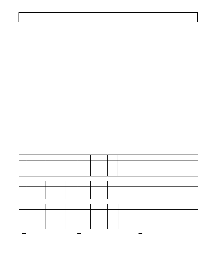
LOGIC T RUT H T ABLE
ADC C HANNE L SE LE C T AND ST ART C ONVE RSION
CS
ADC
/DAC
CHA
/CHB
WR
RD
DB0–DB7
INT
Comments
0
0
0
0
0
0
X
0
1
Note 1
Note 1
Note 1
Note 1
Note 1
Note 1
1
1
1
0
INT
Is Set on Falling Edge of
WR
.
Select ADC Channel A and Start Conversion.
Select ADC Channel B and Start Conversion.
INT
Goes Low at End of Conversion.
RE AD ADC DAT A
CS
ADC
/DAC
CHA
/CHB
WR
RD
DB0–DB7
INT
Comments
0
0
0
X
X
X
X
X
X
X
X
X
ADC Data
ADC Data
High-Z
1
1
1
INT
Is Set High on Falling Edge of
RD
.
ADC Data on Data Bus.
Data Outputs Impedance.
0
WRIT E T O DAC A OR DAC B
CS
ADC
/DAC
CHA
/CHB
WR
RD
DB0–DB7
INT
Comments
0
0
0
0
1
1
1
1
1
X
0
1
0
1
X
1
1
0
0
X
μ
P Data
μ
P Data
ADC Data
ADC Data
High-Z
N/C
N/C
N/C
N/C
N/C
μ
P Writing Data to DACA.
μ
P Writing Data to DACB.
Data from Last ADC Conversion Will Be Written to DACA.
Data from Last ADC Conversion Will Be Written to DACB.
No Operation.
X
NOT ES
1
If
RD
= 1, DB0–DB7 will remain high impedance. If
RD
= 0, DB0–DB7 will output previous ADC data. T he
RD
input should not change during a conversion.
2
X = Don’t Care.
3
N/C = No Change.
相關PDF資料 |
PDF描述 |
|---|---|
| AD7769AN | LC2MOS Analog I/O Port |
| AD7769AP | LC2MOS Analog I/O Port |
| AD7769JN | LC2MOS Analog I/O Port |
| AD7769JP | LC2MOS Analog I/O Port |
| AD7773 | LC MOS COMPLETE EMBEDDED SERVO FRONT ENDS FOR HDD |
相關代理商/技術參數 |
參數描述 |
|---|---|
| AD7769AN | 制造商:AD 制造商全稱:Analog Devices 功能描述:LC2MOS Analog I/O Port |
| AD7769AP | 制造商:AD 制造商全稱:Analog Devices 功能描述:LC2MOS Analog I/O Port |
| AD7769JN | 制造商:AD 制造商全稱:Analog Devices 功能描述:LC2MOS Analog I/O Port |
| AD7769JP | 制造商:Rochester Electronics LLC 功能描述:- Bulk |
| AD7769JP-REEL | 制造商:Rochester Electronics LLC 功能描述:- Tape and Reel |
發布緊急采購,3分鐘左右您將得到回復。