- 您現在的位置:買賣IC網 > PDF目錄373916 > AD7788 (Analog Devices, Inc.) Low Power, 16-/24-Bit Sigma-Delta ADC PDF資料下載
參數資料
| 型號: | AD7788 |
| 廠商: | Analog Devices, Inc. |
| 元件分類: | ADC |
| 英文描述: | Low Power, 16-/24-Bit Sigma-Delta ADC |
| 中文描述: | 低功耗,16-/24-BitΣ-Δ模數轉換器 |
| 文件頁數: | 14/20頁 |
| 文件大小: | 288K |
| 代理商: | AD7788 |
AD7788/AD7789
ADC CIRCUIT INFORMATION
OVERVIEW
The AD7788/AD7789 is a low power ADC that incorporates a
∑- modulator and on-chip digital filtering intended for the
measurement of wide dynamic range, low frequency signals
such as those in pressure transducers, weigh scales, and
temperature measurement applications.
Rev. 0 | Page 14 of 20
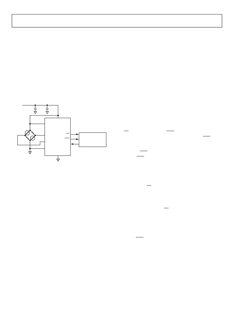
The part has one unbuffered differential input. The device
requires an external reference voltage between 0.1 V and V
DD
.
Figure 10 shows the basic connections required to operate
the part.
03539-0-006
IN+
10
μ
F
0.1
μ
F
IN–
OUT–
POWER
SUPPLY
OUT+
REFIN(+)
CS
DOUT/RDY
SCLK
V
DD
GND
AIN(+)
AIN(–)
REFIN(–)
AD7788/
AD7789
MICROCONTROLLER
Figure 10. Basic Connection Diagram
The output rate of the AD7788/AD7789 (f
ADC
) is 16.6 Hz with
the settling time equal to 2 × t
ADC
(120.4 ms). Normal mode
rejection is the major function of the digital filter. Simultaneous
50 Hz and 60 Hz rejection is optimized as notches are placed at
both 50 Hz and 60 Hz with this update rate (see Figure 6).
NOISE PERFORMANCE
The AD7788/AD7789 has an rms noise of 1.5 μV rms typically,
which corresponds to a peak-to-peak resolution of 16 bits for
the AD7788 and 19 bits (equivalent to an effective resolution of
21.5 bits) for the AD7789. The numbers given are for the bipo-
lar input range with a reference of 2.5 V. The noise was
measured with a differential input voltage of 0 V. The peak-to-
peak resolution figures represent the resolution for which there
will be no code flicker within a six-sigma limit. The output
noise comes from two sources. The first is the electrical noise in
the semiconductor devices (device noise) used in the imple-
mentation of the modulator. The second is quantization noise,
which is added when the analog input is converted into the
digital domain.
DIGITAL INTERFACE
As previously outlined, the AD7788/AD7789’s programmable
functions are controlled using a set of on-chip registers. Data is
written to these registers via the part’s serial interface and read
access to the on-chip registers is also provided by this interface.
All communications with the part must start with a write to the
communications register. After power-on or reset, the device
expects a write to its communications register. The data written
to this register determines whether the next operation is a read
operation or a write operation and also determines to which
register this read or write operation occurs. Therefore, write
access to any of the other registers on the part begins with a
write operation to the communications register followed by a
write to the selected register. A read operation from any other
register (except when continuous read mode is selected) starts
with a write to the communications register followed by a read
operation from the selected register.
The AD7788/AD7789’s serial interface consists of four signals:
CS, DIN, SCLK, and DOUT/RDY. The DIN line is used to
transfer data into the on-chip registers while DOUT/RDY is
used for accessing from the on-chip registers. SCLK is the serial
clock input for the device and all data transfers (either on DIN
or DOUT/RDY) occur with respect to the SCLK signal. The
DOUT/ RDY pin operates as a Data Ready signal also, the line
going low when a new data-word is available in the output reg-
ister. It is reset high when a read operation from the data
register is complete. It also goes high prior to the updating of
the data register to indicate when not to read from the device to
ensure that a data read is not attempted while the register is
being updated. CS is used to select a device. It can be used to
decode the AD7788/AD7789 in systems where several compo-
nents are connected to the serial bus.
Figure 3 and Figure 4 show timing diagrams for interfacing to
the AD7788/AD7789 with CS being used to decode the part.
Figure 3 shows the timing for a read operation from the
AD7788/AD7789’s output shift register while Figure 4 shows
the timing for a write operation to the input shift register. In all
modes except continuous read mode, it is possible to read the
same word from the data register several times even though the
DOUT/RDY line returns high after the first read operation.
However, care must be taken to ensure that the read operations
have been completed before the next output update occurs. In
continuous read mode, the data register can be read only once.
相關PDF資料 |
PDF描述 |
|---|---|
| AD7788ARM | Low Power, 16-/24-Bit Sigma-Delta ADC |
| AD7788ARM-REEL | Low Power, 16-/24-Bit Sigma-Delta ADC |
| AD7789BRM | Low Power, 16-/24-Bit Sigma-Delta ADC |
| AD7788BRM | Low Power, 16-/24-Bit Sigma-Delta ADC |
| AD7788BRM-REEL | Low Power, 16-/24-Bit Sigma-Delta ADC |
相關代理商/技術參數 |
參數描述 |
|---|---|
| AD7788ARM | 功能描述:IC ADC 16BIT SIGMA-DELTA 10-MSOP RoHS:是 類別:集成電路 (IC) >> 數據采集 - 模數轉換器 系列:- 標準包裝:1,000 系列:- 位數:16 采樣率(每秒):45k 數據接口:串行 轉換器數目:2 功率耗散(最大):315mW 電壓電源:模擬和數字 工作溫度:0°C ~ 70°C 安裝類型:表面貼裝 封裝/外殼:28-SOIC(0.295",7.50mm 寬) 供應商設備封裝:28-SOIC W 包裝:帶卷 (TR) 輸入數目和類型:2 個單端,單極 |
| AD7788ARM-REEL | 功能描述:IC ADC 16BIT SIGMA-DELTA 10-MSOP RoHS:否 類別:集成電路 (IC) >> 數據采集 - 模數轉換器 系列:- 標準包裝:2,500 系列:- 位數:16 采樣率(每秒):15 數據接口:MICROWIRE?,串行,SPI? 轉換器數目:1 功率耗散(最大):480µW 電壓電源:單電源 工作溫度:-40°C ~ 85°C 安裝類型:表面貼裝 封裝/外殼:38-WFQFN 裸露焊盤 供應商設備封裝:38-QFN(5x7) 包裝:帶卷 (TR) 輸入數目和類型:16 個單端,雙極;8 個差分,雙極 配用:DC1011A-C-ND - BOARD DELTA SIGMA ADC LTC2494 |
| AD7788ARMZ | 功能描述:IC ADC 16BIT SIGMA-DELTA 10MSOP RoHS:是 類別:集成電路 (IC) >> 數據采集 - 模數轉換器 系列:- 標準包裝:1 系列:microPOWER™ 位數:8 采樣率(每秒):1M 數據接口:串行,SPI? 轉換器數目:1 功率耗散(最大):- 電壓電源:模擬和數字 工作溫度:-40°C ~ 125°C 安裝類型:表面貼裝 封裝/外殼:24-VFQFN 裸露焊盤 供應商設備封裝:24-VQFN 裸露焊盤(4x4) 包裝:Digi-Reel® 輸入數目和類型:8 個單端,單極 產品目錄頁面:892 (CN2011-ZH PDF) 其它名稱:296-25851-6 |
| AD7788ARMZ-REEL | 功能描述:IC ADC 16BIT SIGMA-DELTA 10-MSOP RoHS:是 類別:集成電路 (IC) >> 數據采集 - 模數轉換器 系列:- 標準包裝:2,500 系列:- 位數:16 采樣率(每秒):15 數據接口:MICROWIRE?,串行,SPI? 轉換器數目:1 功率耗散(最大):480µW 電壓電源:單電源 工作溫度:-40°C ~ 85°C 安裝類型:表面貼裝 封裝/外殼:38-WFQFN 裸露焊盤 供應商設備封裝:38-QFN(5x7) 包裝:帶卷 (TR) 輸入數目和類型:16 個單端,雙極;8 個差分,雙極 配用:DC1011A-C-ND - BOARD DELTA SIGMA ADC LTC2494 |
| AD7788BRM | 功能描述:IC ADC 16BIT LP 10-MSOP RoHS:否 類別:集成電路 (IC) >> 數據采集 - 模數轉換器 系列:- 標準包裝:1,000 系列:- 位數:16 采樣率(每秒):45k 數據接口:串行 轉換器數目:2 功率耗散(最大):315mW 電壓電源:模擬和數字 工作溫度:0°C ~ 70°C 安裝類型:表面貼裝 封裝/外殼:28-SOIC(0.295",7.50mm 寬) 供應商設備封裝:28-SOIC W 包裝:帶卷 (TR) 輸入數目和類型:2 個單端,單極 |
發布緊急采購,3分鐘左右您將得到回復。