- 您現在的位置:買賣IC網 > PDF目錄373918 > AD7822BR (ANALOG DEVICES INC) 3 V/5 V, 2 MSPS, 8-Bit, 1-, 4-, 8-Channel Sampling ADCs PDF資料下載
參數資料
| 型號: | AD7822BR |
| 廠商: | ANALOG DEVICES INC |
| 元件分類: | ADC |
| 英文描述: | 3 V/5 V, 2 MSPS, 8-Bit, 1-, 4-, 8-Channel Sampling ADCs |
| 中文描述: | 1-CH 8-BIT FLASH METHOD ADC, PARALLEL ACCESS, PDSO20 |
| 封裝: | MS-013AC, SOIC-20 |
| 文件頁數: | 11/18頁 |
| 文件大小: | 215K |
| 代理商: | AD7822BR |
AD7822/AD7825/AD7829
–11–
REV. A
Figure 16 shows how to power up the AD7822 or AD7825 when
V
DD
is first connected or after the ADCs have been powered
down using the
PD
pin, or the
CONVST
pin, with either the
on-chip or an external reference. When the supplies are first
connected or after the part has been powered down by the
PD
pin, only a rising edge on the
PD
pin will cause the part to
power up. When the part has been powered down using the
CONVST
pin, a rising edge on either the
PD
pin or the
CONVST
pin will power the part up again.
As with the AD7829, when using an external reference with the
AD7822 or AD7825, the falling edge of
CONVST
may occur
before the required power-up time has elapsed, however, if this
is the case, the conversion will not be initiated on the falling edge
of
CONVST
, but rather at the moment when the part has powered
up completely, i.e., after 1
μ
s. If the falling edge of
CONVST
occurs after the required power-up time has elapsed, it is upon
this falling edge that a conversion is initiated. When using the
on-chip reference it is necessary to wait the required power-
up time of approximately 25
μ
s before initiating a conversion;
i.e., a falling edge on
CONVST
may not occur before the
required power-up time has elapsed, when supplies are first
connected to the AD7822 or AD7825, or when the ADCs have
been powered down using the PD pin or the
CONVST
pin as
shown in Figure 16.
V
DD
PD
CONVST
t
POWER-UP
1
m
s
t
POWER-UP
1
m
s
CONVERSION
INITIATED HERE
CONVERSION
INITIATED HERE
V
DD
PD
CONVST
t
POWER-UP
25
m
s
t
POWER-UP
25
m
s
CONVERSION
INITIATED HERE
CONVERSION
INITIATED HERE
EXTERNAL REFERENCE
ON-CHIP REFERENCE
Figure 16. AD7822/AD7825 Power-Up Time
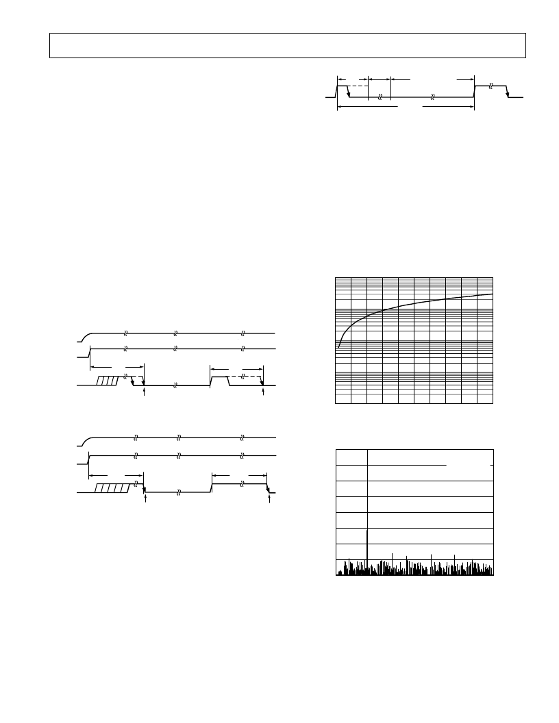
POWER VS. THROUGHPUT
Superior power performance can be achieved by using the auto-
matic power-down (Mode 2) at the end of a conversion—see
Operating Modes section of the data sheet.
Figure 17 shows how the automatic power-down is implemented
using the
CONVST
signal to achieve the optimum power per-
formance for the AD7822, AD7825, and AD7829. The duration
of the
CONVST
pulse is set to be equal to or less than the
power-up time of the devices—see Operating Modes section. As
the throughput rate is reduced, the device remains in its power-
down state longer and the average power consumption over time
drops accordingly.
t
POWER-UP
1
m
s
330ns
t
CONVERT
POWER-DOWN
t
CYCLE
10
m
s @ 100kSPS
CONVST
Figure 17. Automatic Power-Down
For example, if the AD7822 is operated in a continuous sam-
pling mode, with a throughput rate of 100 kSPS and using an
external reference, the power consumption is calculated as fol-
lows. The power dissipation during normal operation is 36 mW,
V
DD
= 3 V. If the power-up time is 1
μ
s and the conversion time
is 330 ns (@ +25
°
C), the AD7822 can be said to dissipate
36 mW for 1.33
μ
s (worst case) during each conversion cycle.
If the throughput rate is 100 kSPS, the cycle time is 10
μ
s
and the average power dissipated during each cycle is (1.33/10)
×
(36 mW) = 4.79 mW.
Figure 18 shows the power vs. throughput rate for automatic
full power-down.
THROUGHPUT – kSPS
100
10
00
500
100
P
1
200
300
400
0.1
50
150
250
350
450
Figure 18. AD7822/AD7825/AD7829 Power vs. Throughput
FREQUENCY – kHz
0
–10
–80
d
–40
–50
–60
–70
–20
–30
0
1
1
1
1
2
2
2
3
3
3
3
4
4
4
5
5
5
5
6
6
6
7
7
7
7
8
8
8
9
9
9
2
5
8
9
2048 POINT FFT
SAMPLING
2MSPS
F
IN
= 200kHz
Figure 19. AD7822/AD7825/AD7829 SNR
相關PDF資料 |
PDF描述 |
|---|---|
| AD7822BRU | 3 V/5 V, 2 MSPS, 8-Bit, 1-, 4-, 8-Channel Sampling ADCs |
| AD7829BN | 2.35V-5.25V, 12 bit, 1MSPS, Serial ADC 6-SOT-23 -40 to 125 |
| AD7829BR | 2.35V-5.25V, 12 bit, 1MSPS, Serial ADC 6-SOT-23 -40 to 125 |
| AD7829BRU | 2.35V-5.25V, 12 bit, 1MSPS, Serial ADC 6-SC70 -40 to 125 |
| AD7827 | 3 V/5 V, 1 MSPS, 8-Bit, Serial Interface Sampling ADC |
相關代理商/技術參數 |
參數描述 |
|---|---|
| AD7822BR-REEL | 功能描述:IC ADC 8BIT 1CH 2MSPS 20-SOIC RoHS:否 類別:集成電路 (IC) >> 數據采集 - 模數轉換器 系列:- 標準包裝:1,000 系列:- 位數:16 采樣率(每秒):45k 數據接口:串行 轉換器數目:2 功率耗散(最大):315mW 電壓電源:模擬和數字 工作溫度:0°C ~ 70°C 安裝類型:表面貼裝 封裝/外殼:28-SOIC(0.295",7.50mm 寬) 供應商設備封裝:28-SOIC W 包裝:帶卷 (TR) 輸入數目和類型:2 個單端,單極 |
| AD7822BR-REEL7 | 制造商:Analog Devices 功能描述:ADC Single Semiflash 2Msps 8-bit Parallel 20-Pin SOIC W T/R 制造商:Analog Devices 功能描述:ADC SGL SEMIFLASH 2MSPS 8BIT PARALLEL 20SOIC W - Tape and Reel |
| AD7822BRU | 功能描述:IC ADC 8BIT 1CH 2MSPS 20TSSOP RoHS:否 類別:集成電路 (IC) >> 數據采集 - 模數轉換器 系列:- 標準包裝:1,000 系列:- 位數:16 采樣率(每秒):45k 數據接口:串行 轉換器數目:2 功率耗散(最大):315mW 電壓電源:模擬和數字 工作溫度:0°C ~ 70°C 安裝類型:表面貼裝 封裝/外殼:28-SOIC(0.295",7.50mm 寬) 供應商設備封裝:28-SOIC W 包裝:帶卷 (TR) 輸入數目和類型:2 個單端,單極 |
| AD7822BRU-REEL | 功能描述:IC ADC 8BIT 1CH 2MSPS 20TSSOP RoHS:否 類別:集成電路 (IC) >> 數據采集 - 模數轉換器 系列:- 標準包裝:1,000 系列:- 位數:16 采樣率(每秒):45k 數據接口:串行 轉換器數目:2 功率耗散(最大):315mW 電壓電源:模擬和數字 工作溫度:0°C ~ 70°C 安裝類型:表面貼裝 封裝/外殼:28-SOIC(0.295",7.50mm 寬) 供應商設備封裝:28-SOIC W 包裝:帶卷 (TR) 輸入數目和類型:2 個單端,單極 |
| AD7822BRU-REEL7 | 功能描述:IC ADC 8BIT 1CH 2MSPS 20TSSOP RoHS:否 類別:集成電路 (IC) >> 數據采集 - 模數轉換器 系列:- 標準包裝:1,000 系列:- 位數:16 采樣率(每秒):45k 數據接口:串行 轉換器數目:2 功率耗散(最大):315mW 電壓電源:模擬和數字 工作溫度:0°C ~ 70°C 安裝類型:表面貼裝 封裝/外殼:28-SOIC(0.295",7.50mm 寬) 供應商設備封裝:28-SOIC W 包裝:帶卷 (TR) 輸入數目和類型:2 個單端,單極 |
發布緊急采購,3分鐘左右您將得到回復。