- 您現在的位置:買賣IC網 > PDF目錄373918 > AD7824TQ (ANALOG DEVICES INC) LC2MOS High Speed 4- & 8-Channel 8-Bit ADCs PDF資料下載
參數資料
| 型號: | AD7824TQ |
| 廠商: | ANALOG DEVICES INC |
| 元件分類: | ADC |
| 英文描述: | LC2MOS High Speed 4- & 8-Channel 8-Bit ADCs |
| 中文描述: | 4-CH 8-BIT FLASH METHOD ADC, PARALLEL ACCESS, CDIP24 |
| 封裝: | 0.300 INCH, SKINNY, CERDIP-24 |
| 文件頁數: | 8/16頁 |
| 文件大小: | 270K |
| 代理商: | AD7824TQ |
AD7824/AD7828
–8–
REV. F
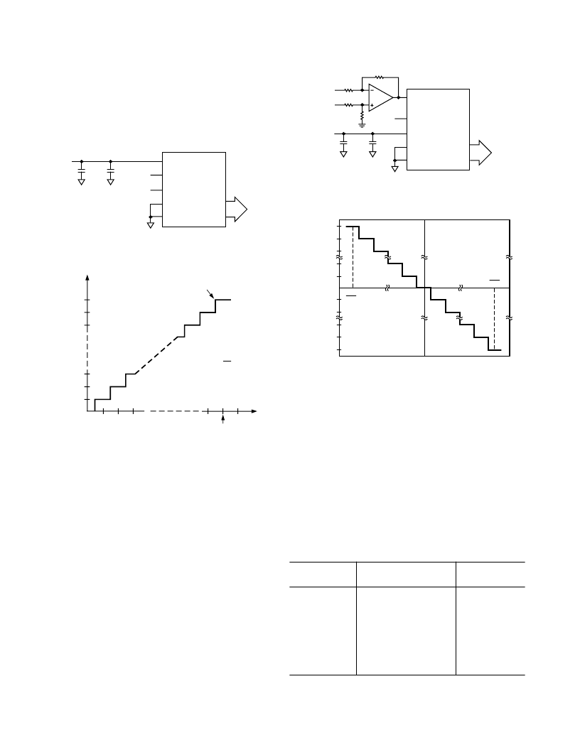
UNIPOLAR OPERATION
The analog input range for any channel of the AD7824/AD7828 is
0 V to 5 V as shown in the unipolar operational diagram of
Figure 10. Figure 11 shows the designed code transitions that
occur midway between successive integer LSB values (i.e., 1/2 LSB,
3/2 LSB, 5/2 LSB, FS 3/2 LSBs). The output code is natural
binary with 1 LSB = FS/256 = (5/256) V = 19.5 mV.
AD7824
*
AD7828
*
AIN1
GND
V
DD
V
REF
(+)
V
REF
(–)
47 F
0.1 F
V
IN
0V TO 5V
5V
ADDITIONAL PINS OMITTED FOR CLARITY.
ONLY CHANNEL 1 SHOWN.
*
DB7
DB0
V
REF
Figure 10. AD7824/AD7828 Unipolar 0 V to 5 V Operation
11111111
11111110
11111101
00000011
00000010
00000001
00000000
FULL-SCALE
TRANSITION
O
1LSB 2LSB 3LSB
FS – 1LSB
FS
0
AIN, INPUT VOLTAGE – LSB
1LSB = 256
Figure 11. Ideal Input/Output Transfer Characteristic for
Unipolar 0 V to 5 V Operation
BIPOLAR OPERATION
The circuit of Figure 12 is designed for bipolar operation. An
AD544 op amp conditions the signal input (V
IN
) so that only
positive voltages appear at AIN1. The closed loop transfer func-
tion of the op amp for the resistor values shown is given below:
(
2 5
.
The analog input range is
±
4 V and the LSB size is 31.25 mV.
The output code is complementary offset binary. The ideal
input/output characteristic is shown in Figure 13.
AIN
V
Volts
IN
1
=
)
0 625
.
AD7824
*
AD7828
*
AIN1
GND
V
DD
V
REF
(+)
V
REF
(–)
47 F
0.1 F
V
IN
5V
ADDITIONAL PINS OMITTED FOR CLARITY.
ONLY CHANNEL 1 SHOWN.
*
DB7
DB0
5V
AD544
5V
40k
27k
25k
12k
Figure 12. AD7824/AD7828 Bipolar
±
4 V Operation
AIN, INPUT VOLTAGE – LSB
11111111
11111110
00000000
0V
O
01111111
01111110
00000010
00000001
10000001
10000000
10000010
11111101
+FS
2
–FS
2
+ 1LSB
FS = 8V
1LSB = FS/256
Figure 13. Ideal Input/Output Transfer Characteristic for
±
4 V Operation
TIMING AND CONTROL
The AD7824/AD7828 has two digital inputs for timing and
control. These are Chip Select (
CS
) and Read (
RD
). A READ
operation brings
CS
and
RD
low, which starts a conversion on
the channel selected by the multiplexer address inputs (see
Table I). There are two modes of operation as outlined by the
timing diagrams of Figures 14 and 15. Mode 0 is designed for
microprocessors that can be driven into a WAIT state. A
READ operation (i.e.,
CS
and
RD
are taken low) starts a con-
version and data is read when conversion is complete. Mode l
does not require microprocessor WAIT states. A READ operation
initiates a conversion and reads the previous conversion results.
Table I. Truth Table for Input Channel Selection
AD7824
A1
AD7828
A1
A0
A2
A0
Channel
0
0
1
1
0
1
0
1
0
0
0
0
1
1
1
1
0
0
1
1
0
0
1
1
0
1
0
1
0
1
0
1
AIN1
AIN2
AIN3
AIN4
AIN5
AIN6
AIN7
AIN8
相關PDF資料 |
PDF描述 |
|---|---|
| AD7824UQ | LC2MOS High Speed 4- & 8-Channel 8-Bit ADCs |
| AD7828KN | LC2MOS High Speed 4- & 8-Channel 8-Bit ADCs |
| AD7828TE | LC2MOS High Speed 4- & 8-Channel 8-Bit ADCs |
| AD7828TQ | LC2MOS High Speed 4- & 8-Channel 8-Bit ADCs |
| AD7824LN | LC2MOS High Speed 4- & 8-Channel 8-Bit ADCs |
相關代理商/技術參數 |
參數描述 |
|---|---|
| AD7824TQ/883B | 制造商:AD 制造商全稱:Analog Devices 功能描述:LC2MOS High Speed 4- & 8-Channel 8-Bit ADCs |
| AD7824UQ | 功能描述:模數轉換器 - ADC High Spd 4-CH 8-Bit CMOS RoHS:否 制造商:Analog Devices 通道數量: 結構: 轉換速率: 分辨率: 輸入類型: 信噪比: 接口類型: 工作電源電壓: 最大工作溫度: 安裝風格: 封裝 / 箱體: |
| AD7824UQ/883 | 制造商:未知廠家 制造商全稱:未知廠家 功能描述:Single-Ended Data Acquisition System |
| AD7824UQ/883B | 制造商:AD 制造商全稱:Analog Devices 功能描述:LC2MOS High Speed 4- & 8-Channel 8-Bit ADCs |
| AD7825 | 制造商:AD 制造商全稱:Analog Devices 功能描述:3 V/5 V, 2 MSPS, 8-Bit, 1-, 4-, 8-Channel Sampling ADCs |
發布緊急采購,3分鐘左右您將得到回復。