- 您現(xiàn)在的位置:買賣IC網(wǎng) > PDF目錄373918 > AD7829BN (ANALOG DEVICES INC) 2.35V-5.25V, 12 bit, 1MSPS, Serial ADC 6-SOT-23 -40 to 125 PDF資料下載
參數(shù)資料
| 型號(hào): | AD7829BN |
| 廠商: | ANALOG DEVICES INC |
| 元件分類: | ADC |
| 英文描述: | 2.35V-5.25V, 12 bit, 1MSPS, Serial ADC 6-SOT-23 -40 to 125 |
| 中文描述: | 8-CH 8-BIT FLASH METHOD ADC, PARALLEL ACCESS, PDIP28 |
| 封裝: | 0.600 INCH, PLASTIC, MS-011AB, DIP-28 |
| 文件頁(yè)數(shù): | 8/18頁(yè) |
| 文件大小: | 215K |
| 代理商: | AD7829BN |
第1頁(yè)第2頁(yè)第3頁(yè)第4頁(yè)第5頁(yè)第6頁(yè)第7頁(yè)當(dāng)前第8頁(yè)第9頁(yè)第10頁(yè)第11頁(yè)第12頁(yè)第13頁(yè)第14頁(yè)第15頁(yè)第16頁(yè)第17頁(yè)第18頁(yè)
AD7822/AD7825/AD7829
–8–
REV. A
ADC TRANSFER FUNCTION
The output coding of the AD7822, AD7825, and AD7829 is
straight binary. The designed code transitions occur at succes-
sive integer LSB values (i.e., 1 LSB, 2 LSBs, etc.). The LSB size
is = V
REF
/256 (V
DD
= 5 V) or the LSB size = (0.8 V
REF
)/256
(V
DD
= 3 V). The ideal transfer characteristic for the AD7822,
AD7825, and AD7829 is shown in Figure 6, below.
11111111
111...110
111...000
10000000
000...111
000...010
000...001
00000000
(V
= 5V)
1LSB = V
REF
/256
(V
= 3V)
1LSB = 0.8V
REF
/256
A
1LSB
V
MID
(V
DD
= 5V) V
MID
–1.25V
(V
DD
= 3V) V
MID
–1V
V
MID
+1.25V–1LSB
V
MID
+1V–1LSB
ANALOG INPUT VOLTAGE
Figure 6. Transfer Characteristic
ANALOG INPUT
The AD7822 has a single input channel and the AD7825 and
AD7829 have four and eight input channels respectively. Each
input channel has an input span of 2.5 V or 2.0 V, depending on
the supply voltage (V
DD
). This input span is automatically set
up by an on-chip “V
DD
Detector” circuit. 5 V operation of the
ADCs is detected when V
DD
exceeds 4.1 V and 3 V operation is
detected when V
DD
falls below 3.8 V. This circuit also possesses
a degree of glitch rejection; for example, a glitch from 5.5 V to
2.7 V up to 60 ns wide will not trip the V
DD
detector.
The V
MID
pin is used to center this input span anywhere in the
range AGND to V
DD
. If no input voltage is applied to V
MID
, i.e.,
if V
MID
is left unconnected, the default input range is AGND
to 2.0 V (V
DD
= 3 V
±
10%) i.e., centered about 1.0 V, or
AGND to 2.5 V (V
DD
= 5 V
±
10%) i.e., centered about 1.25 V.
If, however, an external V
MID
is applied, the analog input range
will be from V
MID
– 1.0 V to V
MID
+ 1.0 V (V
DD
= 3 V
±
10%),
or from V
MID
– 1.25 V to V
MID
+ 1.25 V (V
DD
= 5 V
±
10%).
The range of values of V
MID
that can be applied depends on the
value of V
DD
. For V
DD
= 3 V
±
10%, the range of values that
can be applied to V
MID
is from 1.0 V to V
DD
– 1.0 V and is 1.25 V
to V
DD
– 1.25 V when V
DD
= 5 V
±
10%. Table I shows the rel-
evant ranges of V
MID
and the input span for various values of
V
DD
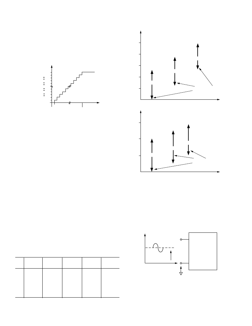
. Figure 7 illustrates the input signal range available with
various values of V
MID
.
Table I.
V
MID
Internal
V
MID
Ext
Max
V
MID
Ext
Min
V
DD
5.5
5.0
4.5
3.3
3.0
2.7
V
IN
Span
3.0 to 5.5
2.5 to 5.0
2.0 to 4.5
1.3 to 3.3
1.0 to 3.0
0.7 to 2.7
V
IN
Span
0 to 2.5
0 to 2.5
0 to 2.5
0 to 2.0
0 to 2.0
0 to 2.0
1.25
1.25
1.25
1.00
1.00
1.00
4.25
3.75
3.25
2.3
2.0
1.7
1.25
1.25
1.25
1.00
1.00
1.00
5V
4V
3V
2V
1V
V
DD
= 5V
INPUT SIGNAL RANGE
FOR VARIOUS V
MID
V
MID
= N/C (1.25V)
V
MID
= 2.5V
V
MID
= 3.75V
3V
2V
1V
V
DD
= 3V
INPUT SIGNAL RANGE
FOR VARIOUS V
MID
V
MID
= N/C (1V)
V
MID
= 1.5V
V
MID
= 2V
Figure 7. Analog Input Span Variation with V
MID
V
MID
may be used to remove offsets in a system by applying the
offset to the V
MID
pin as shown in Figure 8, or it may be used to
accommodate bipolar signals by applying V
MID
to a level-shifting
circuit before V
IN
, as shown in Figure 9. When V
MID
is being
driven by an external source, the source may be directly tied to
the level-shifting circuitry, see Figure 9; however, if the internal
V
MID
, i.e., the default value, is being used as an output, it must
be buffered before applying it to the level-shifting circuitry
as the V
MID
pin has an impedance of approximately 6 k
, see
Figure 10.
V
IN
V
MID
AD7822/
AD7825/
AD7829
V
MID
V
IN
V
MID
Figure 8. Removing Offsets Using V
MID
相關(guān)PDF資料 |
PDF描述 |
|---|---|
| AD7829BR | 2.35V-5.25V, 12 bit, 1MSPS, Serial ADC 6-SOT-23 -40 to 125 |
| AD7829BRU | 2.35V-5.25V, 12 bit, 1MSPS, Serial ADC 6-SC70 -40 to 125 |
| AD7827 | 3 V/5 V, 1 MSPS, 8-Bit, Serial Interface Sampling ADC |
| AD7827BN | 14-Bit 48KSPS DAS with ADC, MUX, PGA and Internal Reference 28-SSOP -40 to 85 |
| AD7827BR | 3 V/5 V, 1 MSPS, 8-Bit, Serial Interface Sampling ADC |
相關(guān)代理商/技術(shù)參數(shù) |
參數(shù)描述 |
|---|---|
| AD7829BNZ | 制造商:Analog Devices 功能描述:ADC Single Semiflash 2Msps 8-bit Parallel 28-Pin PDIP W 制造商:Analog Devices 功能描述:IC 8BIT ADC 7829 DIP28 |
| AD7829BNZ1 | 制造商:AD 制造商全稱:Analog Devices 功能描述:3 V/5 V, 2 MSPS, 8-Bit, 1-/4-/8-Channel Sampling ADCs |
| AD7829BR | 制造商:Rochester Electronics LLC 功能描述:8-CHNL 2MSPS PARALLEL 8-BIT ADC I.C. - Bulk 制造商:Analog Devices 功能描述:IC 8-BIT ADC |
| AD7829BR-REEL | 制造商:Analog Devices 功能描述:ADC Single Semiflash 2Msps 8-bit Parallel 28-Pin SOIC W T/R 制造商:Rochester Electronics LLC 功能描述:8-CHNL 2MSPS PARALLEL 8-BIT ADC I.C. - Tape and Reel |
| AD7829BRREEL7 | 制造商:ANALOG 功能描述:NEW |
發(fā)布緊急采購(gòu),3分鐘左右您將得到回復(fù)。