- 您現在的位置:買賣IC網 > PDF目錄373918 > AD7835 (Analog Devices, Inc.) 14-Bit Quad DAC(14位四D/A轉換器) PDF資料下載
參數資料
| 型號: | AD7835 |
| 廠商: | Analog Devices, Inc. |
| 英文描述: | 14-Bit Quad DAC(14位四D/A轉換器) |
| 中文描述: | 14位四路DAC(14位四的D / A轉換器) |
| 文件頁數: | 9/16頁 |
| 文件大小: | 416K |
| 代理商: | AD7835 |
AD7834/AD7835
REV. A
–9–
Table I. D23 Control
D23
Control Function
0
1
Ignore following 23 bits of information.
Use following 23 bits of address and
data as normal.
D22 and D21:
Decoded to select one of the four DAC channels
within a device. The truth table for D22 and D21 is as shown
below in Table II.
Table II. D22, D21 Control
D22
0
0
1
1
D21
0
1
0
1
Control Function
Select Channel 1
Select Channel 2
Select Channel 3
Select Channel 4
D20–D16
: Determines the package address. The five address
bits allow up to 32 separate packages to be individually de-
coded. Successful decoding is accomplished when these five bits
match up with the five hardwired pins on the physical package.
D15–D0
: DAC Data to be loaded into identified DAC Input
Register. This data must have two leading 0s followed by 14 bits
of data, MSB first. The MSB is in location D13 of the 24-bit
data stream.
Data Loading—AD7835, Parallel Loading Device
Data can be loaded into the AD7835 in either straight 14-bit
wide words or in two 8-bit bytes.
In systems which can transfer 14-bit wide data, the
BYSHF
input should be hardwired to V
CC
. This sets up the AD7835
as a straight 14-bit parallel-loading DAC.
In 8-bit bus systems where it is required to transfer data in two
bytes, it is necessary to have the
BYSHF
input under logic con-
trol. In such a system the top 6 pins of the device data bus,
DB8–DB13, must be hardwired to DGND. New low byte data
is loaded into the lower 8 places of the selected input register by
carrying out a write operation while holding
BYSHF
high. A
second write operation is subsequently executed with
BYSHF
low and the 6 MSBs on the DB0–DB5 inputs (DB5 = MSB).
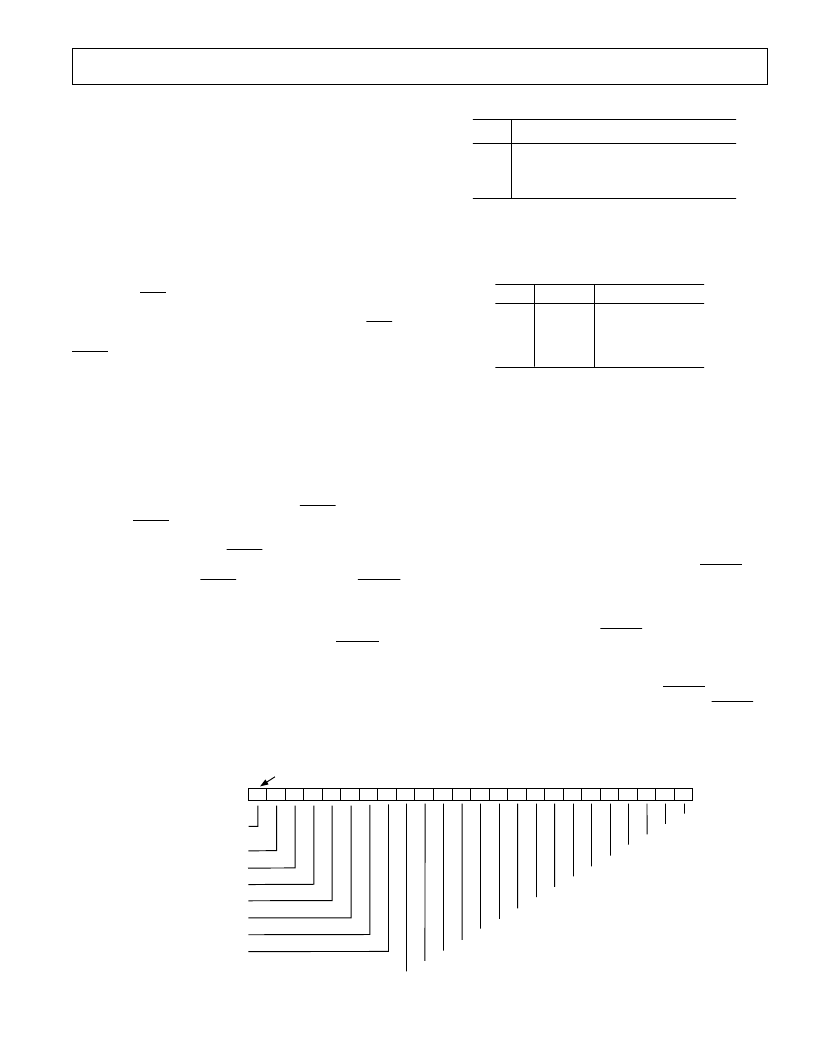
D23 D22 D21 D20 D19 D18 D17 D16 D15 D14 D13 D12 D11 D10
D9
D8
D7
D6
D5
D4
D3
D2
D1
D0
NOTE: D23 IS THE FIRST BIT TRANSMITTED IN THE SERIAL WORD.
CONTROL BIT TO USE/IGNORE
FOLLOWING 23 BITS OF INFORMATION
CHANNEL ADDRESS MSB, D1
CHANNEL ADDRESS LSB, D2
PACKAGE ADDRESS MSB, PA4
PACKAGE ADDRESS, PA3
PACKAGE ADDRESS, PA2
PACKAGE ADDRESS, PA1
PACKAGE ADDRESS LSB, PA0
LSB, DB0
SECOND LSB, DB1
THIRD LSB, DB2
DB3
DB4
DB5
DB6
DB7
DB8
DB9
DB10
THIRD MSB, DB11
SECOND MSB, DB12
MSB, DB13
SECOND LEADING ZERO
FIRST LEADING ZERO
Figure 12. Bit Assignments for 24-Bit Data Stream of AD7834
GENERAL DESCRIPTION
DAC Architecture—General
Each channel consists of a segmented 14-bit R-2R voltage-mode
DAC. The full- scale output voltage range is equal to the entire
reference span of V
REF
(+) – V
REF
(–). The DAC coding is
straight binary; all 0s produces an output of V
REF
(–); all 1s pro-
duces an output of V
REF
(+) – 1 LSB.
The analog output voltage of each DAC channel reflects the
contents of its own DAC latch. Data is transferred from the ex-
ternal bus to the input register of each DAC latch on a per
channel basis. The AD7835 has a feature whereby using the A2
pin, data can be transferred from the input data bus to all four
input registers simultaneously.
Bringing the
CLR
line low switches all the signal outputs,
V
OUT
1 to V
OUT
4, to the voltage level on the DSG pin. The sig-
nal outputs are held at this level after the removal of the
CLR
signal and will not switch back to the DAC outputs until the
LDAC
signal is exercised.
Data Loading—AD7834, Serial Input Device
A write operation transfers 24 bits of data to the AD7834. The
first 8 bits are control data and the remaining 16 bits are DAC
data (see Figure 12). The control data identifies the DAC chan-
nel to be updated with new data and which of 32 possible pack-
ages the DAC resides in. In any communication with the device
the first 8 bits must always be control data.
Note that the DAC output voltages, V
OUT
1 to V
OUT
4, can be
updated to reflect new data in the DAC input registers in one of
two ways. The first method normally keeps
LDAC
high and
only pulses
LDAC
low momentarily to update all DAC latches
simultaneously with the contents of their respective input regis-
ters. The second method ties
LDAC
low, and channel updating
occurs on a per channel basis after new data has been clocked
into the AD7834. With
LDAC
low, the rising edge of
FSYNC
transfers the new data directly into the DAC latch, updating the
analog output voltage.
Data being shifted into the AD7834 enters a 24-bit long shift
register. If more than 24 bits are clocked in before
FSYNC
goes
high, the last 24 bits transmitted are used as the control data
and DAC data.
Individual bit functions are discussed below.
D23
: Determines whether the following 23-bits of address and
data should be used or should be ignored. This is effectively a
software Chip Select bit. D23 is the first bit to be transmitted in
the 24-bit long word.
相關PDF資料 |
PDF描述 |
|---|---|
| AD7837AR | LC2MOS Complete, Dual 12-Bit MDACs |
| AD7837BN | LC2MOS Complete, Dual 12-Bit MDACs |
| AD7837BQ | 2.7V-5.25V Digital, 5V Analog, 14 Bit, 1.25 MSPS, Serial ADC w/Ref 48-TQFP -40 to 85 |
| AD7837BR | LC2MOS Complete, Dual 12-Bit MDACs |
| AD7837SQ | 2.7V-5.25V Digital, 5V Analog, 14 Bit, 1.25 MSPS, Serial ADC w/Ref 48-TQFP -40 to 85 |
相關代理商/技術參數 |
參數描述 |
|---|---|
| AD7835AP | 功能描述:IC DAC 14BIT QUAD PARA 44-PLCC RoHS:否 類別:集成電路 (IC) >> 數據采集 - 數模轉換器 系列:- 產品培訓模塊:Lead (SnPb) Finish for COTS Obsolescence Mitigation Program 標準包裝:1,000 系列:- 設置時間:1µs 位數:8 數據接口:串行 轉換器數目:8 電壓電源:雙 ± 功率耗散(最大):941mW 工作溫度:0°C ~ 70°C 安裝類型:表面貼裝 封裝/外殼:24-SOIC(0.295",7.50mm 寬) 供應商設備封裝:24-SOIC W 包裝:帶卷 (TR) 輸出數目和類型:8 電壓,單極 采樣率(每秒):* |
| AD7835AP-REEL | 制造商:Analog Devices 功能描述:DAC 4-CH R-2R 14-bit 44-Pin PLCC T/R 制造商:Analog Devices 功能描述:DAC 4-CH R-2R 14BIT 44PLCC - Tape and Reel 制造商:Rochester Electronics LLC 功能描述:QUAD 14-BIT PARALLEL DAC I.C. - Tape and Reel |
| AD7835APZ | 功能描述:IC DAC 14BIT QUAD PARALL 44PLCC RoHS:是 類別:集成電路 (IC) >> 數據采集 - 數模轉換器 系列:- 標準包裝:1 系列:- 設置時間:4.5µs 位數:12 數據接口:串行,SPI? 轉換器數目:1 電壓電源:單電源 功率耗散(最大):- 工作溫度:-40°C ~ 125°C 安裝類型:表面貼裝 封裝/外殼:8-SOIC(0.154",3.90mm 寬) 供應商設備封裝:8-SOICN 包裝:剪切帶 (CT) 輸出數目和類型:1 電壓,單極;1 電壓,雙極 采樣率(每秒):* 其它名稱:MCP4921T-E/SNCTMCP4921T-E/SNRCTMCP4921T-E/SNRCT-ND |
| AD7835APZ-REEL | 功能描述:IC DAC 14BIT QUAD PARALL 44PLCC RoHS:是 類別:集成電路 (IC) >> 數據采集 - 數模轉換器 系列:- 標準包裝:2,400 系列:- 設置時間:- 位數:18 數據接口:串行 轉換器數目:3 電壓電源:模擬和數字 功率耗散(最大):- 工作溫度:-40°C ~ 85°C 安裝類型:表面貼裝 封裝/外殼:36-TFBGA 供應商設備封裝:36-TFBGA 包裝:帶卷 (TR) 輸出數目和類型:* 采樣率(每秒):* |
| AD7835AS | 制造商:Analog Devices 功能描述:DAC 4-CH R-2R 14-bit 44-Pin MQFP 制造商:Rochester Electronics LLC 功能描述:QUAD 14-BIT PARALLEL DAC I.C. - Bulk 制造商:Analog Devices 功能描述:IC 14-BIT DAC |
發布緊急采購,3分鐘左右您將得到回復。