- 您現在的位置:買賣IC網 > PDF目錄373918 > AD7837BN (ANALOG DEVICES INC) LC2MOS Complete, Dual 12-Bit MDACs PDF資料下載
參數資料
| 型號: | AD7837BN |
| 廠商: | ANALOG DEVICES INC |
| 元件分類: | DAC |
| 英文描述: | LC2MOS Complete, Dual 12-Bit MDACs |
| 中文描述: | DUAL, PARALLEL, WORD INPUT LOADING, 3 us SETTLING TIME, 12-BIT DAC, PDIP24 |
| 封裝: | 0.300 INCH, PLASTIC, DIP-24 |
| 文件頁數: | 2/12頁 |
| 文件大小: | 187K |
| 代理商: | AD7837BN |
REV. C
–2–
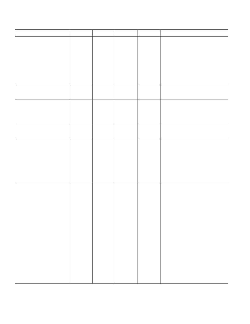
AD7837/AD7847–SPECIFICATIONS
1
= O V. V
REFA
= V
REFB
= +10 V, R
L
= 2 k , C
L
= 100 pF [V
OUT
connected to R
FB
AD7837]. All specifications T
MIN
to T
MAX
unless otherwise noted.)
(V
DD
= +15 V 5%, V
SS
= –15 V 5%, AGNDA = AGNDB = DGND
Parameter
A Version
B Version
S Version
Units
Test Conditions/Comments
STATIC PERFORMANCE
Resolution
Relative Accuracy
2
Differential Nonlinearity
2
Zero Code Offset Error
2
@ +25
°
C
T
MIN
to T
MAX
Gain Error
2
@ +25
°
C
T
MIN
to T
MAX
12
±
1
±
1
12
±
1/2
±
1
12
±
1
±
1
Bits
LSB max
LSB max
Guaranteed Monotonic
±
2
±
4
±
2
±
3
±
2
±
4
mV max
mV max
DAC Latch Loaded with All 0s
Temperature Coefficient =
±
5
μ
V/
°
C typ
±
4
±
5
±
2
±
3
±
4
±
5
LSB max
LSB max
DAC Latch Loaded with All 1s
Temperature Coefficient =
±
2 ppm of
FSR/
°
C typ
REFERENCE INPUTS
V
REF
Input Resistance
V
REFA
, V
REFB
Resistance Matching
8/13
±
2
8/13
±
2
8/13
±
2
k
min/max
% max
Typical Input Resistance = 10 k
Typically
±
0.25%
DIGITAL INPUTS
Input High Voltage, V
INH
Input Low Voltage, V
INL
Input Current
Input Capacitance
3
2.4
0.8
±
1
8
2.4
0.8
±
1
8
2.4
0.8
±
1
8
V min
V max
μ
A max
pF max
Digital Inputs at 0 V and V
DD
ANALOG OUTPUTS
DC Output Impedance
Short Circuit Current
0.2
11
0.2
11
0.2
11
typ
mA typ
V
OUT
Connected to AGND
POWER REQUIREMENTS
4
V
DD
Range
V
SS
Range
Power Supply Rejection
Gain/
V
DD
Gain/
V
SS
I
DD
14.25/15.75
–14.25/–15.75
14.25/15.75
–14.25/–15.75 –14.25/–15.75
14.25/15.75
V min/max
V min/max
±
0.01
±
0.01
8
±
0.01
±
0.01
8
±
0.01
±
0.01
8
% per % max
% per % max
mA max
V
DD
= 15 V
±
5%, V
REF
= –10 V
V
SS
= –15 V
±
5%, V
REF
= +10 V
Outputs Unloaded. Inputs at Thresholds.
Typically 5 mA
Outputs Unloaded. Inputs at Thresholds.
Typically 3 mA
I
SS
6
6
6
mA max
AC CHARACTERISTICS
2, 3
Voltage Output Settling Time
3
5
3
5
3
5
μ
s typ
μ
s max
Settling Time to Within
±
1/2 LSB of Final
Value. DAC Latch Alternately Loaded
with All 0s and All 1s
Slew Rate
Digital-to-Analog Glitch Impulse
Channel-to-Channel Isolation
V
REFA
to V
OUTB
11
10
11
10
11
10
V/
μ
s typ
nV secs typ
1 LSB Change Around Major Carry
–95
–95
–95
dB typ
V
REFA
= 20 V p-p, 10 kHz Sine Wave.
DAC Latches Loaded with All 0s
V
REFB
= 20 V p-p, 10 kHz Sine Wave.
DAC Latches Loaded with All 0s
V
REF
= 20 V p-p, 10 kHz Sine Wave.
DAC Latch Loaded with All 0s
V
REF
= 100 mV p-p Sine Wave. DAC
Latch Loaded with All 1s
V
REF
= 20 V p-p Sine Wave. DAC
Latch Loaded with All 1s
V
REF
= 6 V rms, 1 kHz. DAC Latch
Loaded with All 1s
Code Transition from All 0s to All 1s and
Vice Versa
See Typical Performance Graphs
Amplifier Noise and Johnson Noise of R
FB
V
REFB
to V
OUTA
–95
–95
–95
dB typ
Multiplying Feedthrough Error
–90
–90
–90
dB typ
Unity Gain Small Signal BW
750
750
750
kHz typ
Full Power BW
175
175
175
kHz typ
Total Harmonic Distortion
–88
–88
–88
dB typ
Digital Crosstalk
1
1
1
nV secs typ
Output Noise Voltage @ +25
°
C
(0.1 Hz to 10 Hz)
Digital Feedthrough
2
1
2
1
2
1
μ
V rms typ
nV secs typ
NOTES
1
Temperature ranges are as follows: A, B Versions, –40
°
C to +85
°
C; S Version, –55
°
C to +125
°
C.
2
See Terminology.
3
Guaranteed by design and characterization, not production tested.
4
The Devices are functional with V
DD
/V
SS
=
±
12 V (See typical performance graphs.).
Specifications subject to change without notice.
相關PDF資料 |
PDF描述 |
|---|---|
| AD7837BQ | 2.7V-5.25V Digital, 5V Analog, 14 Bit, 1.25 MSPS, Serial ADC w/Ref 48-TQFP -40 to 85 |
| AD7837BR | LC2MOS Complete, Dual 12-Bit MDACs |
| AD7837SQ | 2.7V-5.25V Digital, 5V Analog, 14 Bit, 1.25 MSPS, Serial ADC w/Ref 48-TQFP -40 to 85 |
| AD7847 | LC2MOS Complete, Dual 12-Bit MDACs |
| AD7847AN | LC2MOS Complete, Dual 12-Bit MDACs |
相關代理商/技術參數 |
參數描述 |
|---|---|
| AD7837BN/883B | 制造商:AD 制造商全稱:Analog Devices 功能描述:LC2MOS Complete, Dual 12-Bit MDACs |
| AD7837BN883B | 制造商:AD 制造商全稱:Analog Devices 功能描述:LC2MOS Complete, Dual 12-Bit MDACs |
| AD7837BN-883B | 制造商:AD 制造商全稱:Analog Devices 功能描述:LC2MOS Complete, Dual 12-Bit MDACs |
| AD7837BNN | 制造商:AD 制造商全稱:Analog Devices 功能描述:LC2MOS Complete, Dual 12-Bit MDACs |
| AD7837BNQ | 制造商:AD 制造商全稱:Analog Devices 功能描述:LC2MOS Complete, Dual 12-Bit MDACs |
發布緊急采購,3分鐘左右您將得到回復。