- 您現在的位置:買賣IC網 > PDF目錄373919 > AD7843ARQ-REEL7 (ANALOG DEVICES INC) Touch Screen Digitizer PDF資料下載
參數資料
| 型號: | AD7843ARQ-REEL7 |
| 廠商: | ANALOG DEVICES INC |
| 元件分類: | 消費家電 |
| 英文描述: | Touch Screen Digitizer |
| 中文描述: | SPECIALTY CONSUMER CIRCUIT, PDSO16 |
| 封裝: | MO-137AB, QSOP-16 |
| 文件頁數: | 12/16頁 |
| 文件大小: | 193K |
| 代理商: | AD7843ARQ-REEL7 |
REV. 0
AD7843
–12–
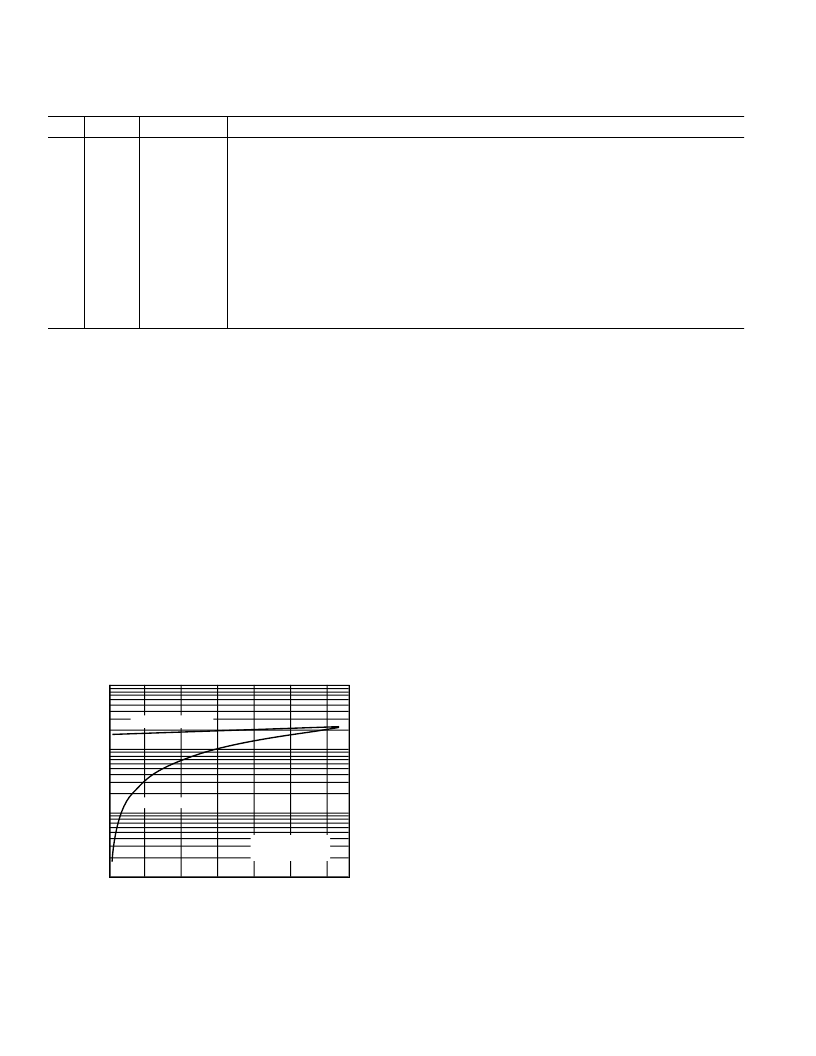
POWER VS. THROUGHPUT RATE
By using the power-down options on the AD7843 when not con-
verting, the average power consumption of the device decreases at
lower throughput rates. Figure 8 shows how, as the through-
put rate is reduced while maintaining the DCLK frequency at
2 MHz, the device remains in its power-down state longer and
the average current consumption over time drops accordingly.
For example, if the AD7843 is operated in a 24 DCLK continu-
ous sampling mode, with a throughput rate of 10 kSPS and a
SCLK of 2 MHz, and the device is placed in the power-down
mode between conversions, (PD0, PD1 = 0, 0), the current
consumption is calculated as follows. The power dissipation
during normal operation is typically 210
μ
A (V
CC
= 2.7 V). The
power-up time of the ADC is instantaneous, so when the part
is converting it will consume 210
μ
A. In this mode of operation
the part powers up on the 4th falling edge of DCLK after the
start bit has been recognized. It goes back into power-down at
the end of conversion on the 20th falling edge of DCLK. This
means the part will consume 210
μ
A for 16 DCLK cycles only,
8
μ
s, during each conversion cycle. With a throughput rate of
10 kSPS, the cycle time is 100
μ
s and the average power dissi-
pated during each cycle is (8/100)
×
(210
μ
A) = 16.8
μ
A.
THROUGHPUT
–
kSPS
1000
S
–
120
100
10
1
60
40
20
0
80
100
f
DCLK
= 16 f
SAMPLE
f
DCLK
= 2MHz
V
CC
= 2.7V
T
A
=
–
40 C to +85 C
Figure 8. Supply Current vs. Throughput (
μ
A)
SERIAL INTERFACE
Figure 9 shows the typical operation of the serial interface of the
AD7843. The serial clock provides the conversion clock and
also controls the transfer of information to and from the AD7843.
One complete conversion can be achieved with twenty-four
DCLK cycles.
The
CS
signal initiates the data transfer and conversion process.
The falling edge of
CS
takes the BUSY output and the serial
bus out of three-state. The first eight DCLK cycles are used to
write to the Control Register via the DIN pin. The Control
Register is updated in stages as each bit is clocked in and once
the converter has enough information about the following con-
version to set the input multiplexer and switches appropriately,
the converter enters the acquisition mode and if required, the
internal switches are turned on. During the acquisition mode
the reference input data is updated. After the three DCLK
cycles of acquisition, the control word is complete (the power
management bits are now updated) and the converter enters the
conversion mode. At this point the track and hold goes into hold
mode and the input signal is sampled and the BUSY output
goes high (BUSY will return low on the next falling edge of
DCLK). The internal switches may also turn off at this point if
in single-ended mode.
The next 12 DCLK cycles are used to perform the conversion
and to clock out the conversion result. If the conversion is
ratiometric (SER/
DFR
set low) the internal switches are on
during the conversion. A thirteenth DCLK cycle is needed to
allow the DSP/micro to clock in the LSB. Three more DCLK
cycles will clock out the three trailing zeroes and complete the
twenty four DCLK transfer. The twenty-four DCLK cycles may
be provided from a DSP or via three bursts of eight clock cycles
from a microcontroller.
Table III. Power Management Options
PD1
PD0
PENIRQ
Description
0
0
Enabled
This configuration will result in power-down of the device between conversions. The AD7843
will only power down between conversions. Once PD1 and PD0 have been set to 0, 0, the
conversion will be performed first and the AD7843 will power down upon completion of that
conversion. At the start of the next conversion, the ADC instantly powers up to full power. This
means there is no need for additional delays to ensure full operation and the very first conversion
is valid. The Y– switch is ON while in power-down.
This configuration will result in the same behavior as when PD1 and PD0 have been programmed
with 0, 0, except that
PENIRQ
is disabled. The Y– switch is OFF while in power-down.
This configuration will result in keeping the AD7843 permanently powered up with the
PENIRQ
enabled.
This configuration will result in keeping the AD7843 always powered up with the
PENIRQ
disabled.
0
1
Disabled
1
0
Enabled
1
1
Disabled
相關PDF資料 |
PDF描述 |
|---|---|
| AD7845 | LC2MOS Complete 12-Bit Multiplying DAC |
| AD7845AQ | LC2MOS Complete 12-Bit Multiplying DAC |
| AD7845AR | LC2MOS Complete 12-Bit Multiplying DAC |
| AD7845BQ | LC2MOS Complete 12-Bit Multiplying DAC |
| AD7845BR | LC2MOS Complete 12-Bit Multiplying DAC |
相關代理商/技術參數 |
參數描述 |
|---|---|
| AD7843ARQZ | 功能描述:IC ADC 12BIT TOUCHSCREEN 16-QSOP RoHS:是 類別:集成電路 (IC) >> 數據采集 - 觸摸屏控制器 系列:- 標準包裝:96 系列:- 類型:- 觸摸面板接口:- 輸入數/鍵:- 分辨率(位):- 評估套件:* 數據接口:- 數據速率/采樣率 (SPS,BPS):- 電壓基準:- 電源電壓:- 電流 - 電源:- 工作溫度:- 安裝類型:表面貼裝 封裝/外殼:16-TSSOP(0.173",4.40mm 寬) 供應商設備封裝:16-TSSOP 包裝:帶卷 (TR) |
| AD7843ARQZ2 | 制造商:AD 制造商全稱:Analog Devices 功能描述:Touch Screen Digitizer |
| AD7843ARQZ-REEL | 功能描述:IC ADC 12BIT TOUCHSCREEN 16-QSOP RoHS:是 類別:集成電路 (IC) >> 數據采集 - 觸摸屏控制器 系列:- 標準包裝:96 系列:- 類型:- 觸摸面板接口:- 輸入數/鍵:- 分辨率(位):- 評估套件:* 數據接口:- 數據速率/采樣率 (SPS,BPS):- 電壓基準:- 電源電壓:- 電流 - 電源:- 工作溫度:- 安裝類型:表面貼裝 封裝/外殼:16-TSSOP(0.173",4.40mm 寬) 供應商設備封裝:16-TSSOP 包裝:帶卷 (TR) |
| AD7843ARQZ-REEL2 | 制造商:AD 制造商全稱:Analog Devices 功能描述:Touch Screen Digitizer |
| AD7843ARQZ-REEL7 | 功能描述:IC ADC 12BIT TOUCHSCREEN 16-QSOP RoHS:是 類別:集成電路 (IC) >> 數據采集 - 觸摸屏控制器 系列:- 標準包裝:96 系列:- 類型:- 觸摸面板接口:- 輸入數/鍵:- 分辨率(位):- 評估套件:* 數據接口:- 數據速率/采樣率 (SPS,BPS):- 電壓基準:- 電源電壓:- 電流 - 電源:- 工作溫度:- 安裝類型:表面貼裝 封裝/外殼:16-TSSOP(0.173",4.40mm 寬) 供應商設備封裝:16-TSSOP 包裝:帶卷 (TR) |
發布緊急采購,3分鐘左右您將得到回復。