- 您現在的位置:買賣IC網 > PDF目錄373919 > AD7843ARU-REEL7 (ANALOG DEVICES INC) Touch Screen Digitizer PDF資料下載
參數資料
| 型號: | AD7843ARU-REEL7 |
| 廠商: | ANALOG DEVICES INC |
| 元件分類: | 消費家電 |
| 英文描述: | Touch Screen Digitizer |
| 中文描述: | SPECIALTY CONSUMER CIRCUIT, PDSO16 |
| 封裝: | MS-153AB, TSSOP-16 |
| 文件頁數: | 8/16頁 |
| 文件大小: | 193K |
| 代理商: | AD7843ARU-REEL7 |
REV. 0
AD7843
–8–
CIRCUIT INFORMATION
The AD7843 is a fast, low-power, 12-bit, single supply, A/D
converter. The AD7843 can be operated from a 2.2 V to 5.25 V
supply. When operated from either a 5 V supply or a 3 V supply,
the AD7843 is capable of throughput rates of 125 kSPS when
provided with a 2 MHz clock.
The AD7843 provides the user with an on-chip track/hold,
multiplexer, A/D converter, and serial interface housed in a tiny
16-lead QSOP or TSSOP package, which offers the user consid-
erable space-saving advantages over alternative solutions. The
serial clock input (DCLK) accesses data from the part but also
provides the clock source for the successive-approximation A/D
converter. The analog input range is 0 V to V
REF
(where the
externally-applied V
REF
can be between 1 V and V
CC
).
The analog input to the ADC is provided via an on-chip multi-
plexer. This analog input may be any one of the X and Y panel
coordinates. The multiplexer is configured with low resistance
switches that allow an unselected ADC input channel to provide
power and an accompanying pin to provide ground for an exter-
nal device. For some measurements the on-resistance of the
switches may present a source of error. However, with a dif-
ferential input to the converter and a differential reference
architecture this error can be negated.
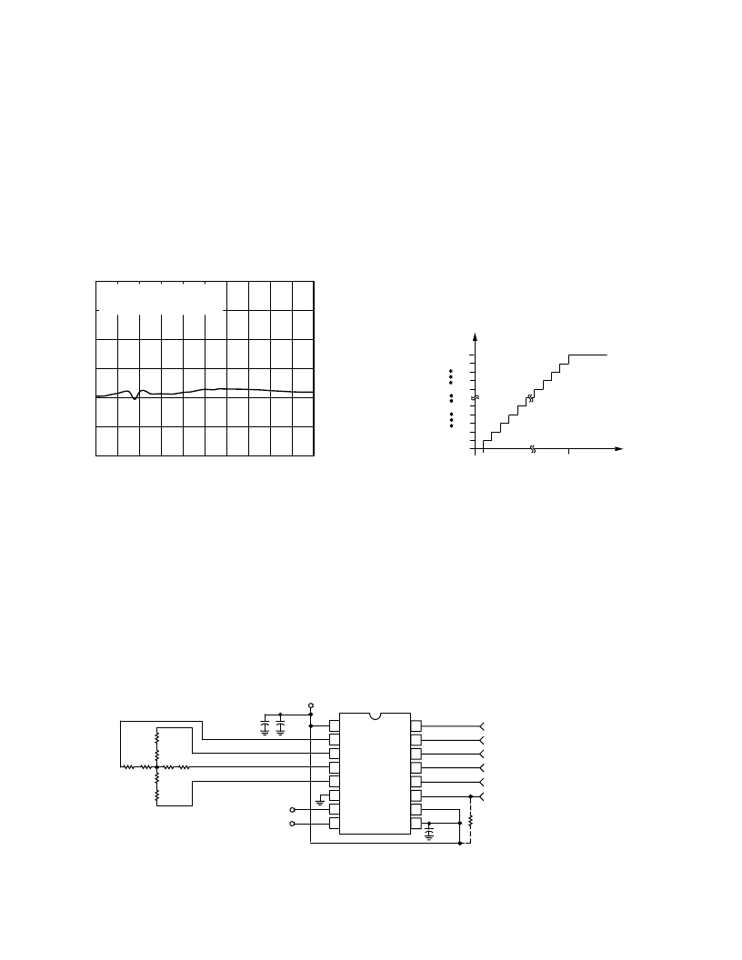
ADC TRANSFER FUNCTION
The output coding of the AD7843 is straight binary. The
designed code transitions occur at successive integer LSB values
(i.e., 1 LSB, 2 LSBs, etc.). The LSB size is = V
REF
/4096. The ideal
transfer characteristic for the AD7843 is shown in Figure 2 below.
000...000
0V
A
ANALOG INPUT
111...111
111...110
000...001
000...010
111...000
011...111
1LSB
+V
REF
–
1LSB
1LSB = V
REF
/4096
Figure 2. AD7843 Transfer Characteristic
TYPICAL CONNECTION DIAGRAM
Figure 3 shows a typical connection diagram for the AD7843 in
a touch screen control application. The AD7843 requires an exter-
nal reference and an external clock. The external reference can
be any voltage between 1 V and V
CC
. The value of the reference
voltage will set the input range of the converter. The conversion
result is output MSB first followed by the remaining eleven bits
and three trailing zeroes depending on the number of clocks used
per conversion, see the Serial Interface section. For applications
where power consumption is of concern, the power management
option should be used to improve power performance. See
Table III for the available power management options.
16
15
14
13
12
11
9
8
1
2
3
4
7
6
5
AD7843
CS
DIN
DCLK
V
REF
+V
CC
GND
DOUT
X+
IN3
IN4
10
BUSY
+V
CC
PENIRQ
X
–
Y+
Y
–
SERIAL/CONVERSION CLOCK
CHIP SELECT
SERIAL DATA IN
CONVERTER STATUS
SERIAL DATA OUT
PEN INTERRUPT
AUXILIARY INPUTS
0.1 F
1 F TO 10 F
(OPTIONAL)
2.2V TO 5V
100k
(OPTIONAL)
0.1 F
TOUCH
SCREEN
Figure 3. Typical Application Circuit
TPC 12 shows a typical FFT plot for the auxiliary channels of
the AD7843 at 125 kHz sample rate and 15 kHz input frequency.
TPC 13 shows the power supply rejection ratio versus V
CC
supply frequency for the AD7843. The power supply rejection
ratio is defined as the ratio of the power in the ADC output at
full-scale frequency f, to the power of a 100 mV sine wave applied
to the ADC V
CC
supply of frequency f
S
:
PSRR
(
dB
)
=
10 log
(
Pf/Pfs
)
Pf
= Power at frequency f in ADC output,
Pfs
= power at fre-
quency f
S
coupled onto the ADC V
CC
supply. Here a 100 mV
peak-to-peak sine wave is coupled onto the V
CC
supply. Decou-
pling capacitors of 10
μ
F and 0.1
μ
F were used on the supply.
V
CC
RIPPLE FREQUENCY
–
kHz
0
P
–
100
–
60
–
80
–
100
–
120
60
40
30
20
10
0
–
20
–
40
80
50
70
90
V
= 3V, V
= 2.5V
100mV p-p SINEWAVE ON +V
CC
f
SAMPLE
= 125kHz, f
IN
= 20kHz
TPC 13. AC PSRR vs. Supply Ripple Frequency
相關PDF資料 |
PDF描述 |
|---|---|
| AD7843ARQ-REEL | Touch Screen Digitizer |
| AD7843ARQ-REEL7 | Touch Screen Digitizer |
| AD7845 | LC2MOS Complete 12-Bit Multiplying DAC |
| AD7845AQ | LC2MOS Complete 12-Bit Multiplying DAC |
| AD7845AR | LC2MOS Complete 12-Bit Multiplying DAC |
相關代理商/技術參數 |
參數描述 |
|---|---|
| AD7843ARUZ | 功能描述:IC ADC 12BIT TOUCHSCREEN 16TSSOP RoHS:是 類別:集成電路 (IC) >> 數據采集 - 觸摸屏控制器 系列:- 標準包裝:96 系列:- 類型:- 觸摸面板接口:- 輸入數/鍵:- 分辨率(位):- 評估套件:* 數據接口:- 數據速率/采樣率 (SPS,BPS):- 電壓基準:- 電源電壓:- 電流 - 電源:- 工作溫度:- 安裝類型:表面貼裝 封裝/外殼:16-TSSOP(0.173",4.40mm 寬) 供應商設備封裝:16-TSSOP 包裝:帶卷 (TR) |
| AD7843ARUZ | 制造商:Analog Devices 功能描述:IC, ADC, 12BIT, 125KSPS, TSSOP-16 |
| AD7843ARUZ-REEL7 | 功能描述:IC ADC 12BIT TOUCHSCREEN 16TSSOP RoHS:是 類別:集成電路 (IC) >> 數據采集 - 觸摸屏控制器 系列:- 標準包裝:96 系列:- 類型:- 觸摸面板接口:- 輸入數/鍵:- 分辨率(位):- 評估套件:* 數據接口:- 數據速率/采樣率 (SPS,BPS):- 電壓基準:- 電源電壓:- 電流 - 電源:- 工作溫度:- 安裝類型:表面貼裝 封裝/外殼:16-TSSOP(0.173",4.40mm 寬) 供應商設備封裝:16-TSSOP 包裝:帶卷 (TR) |
| AD7845 | 制造商:AD 制造商全稱:Analog Devices 功能描述:LC2MOS Complete 12-Bit Multiplying DAC |
| AD7845AQ | 功能描述:IC DAC 12BIT MULT LC2MOS 24-CDIP RoHS:否 類別:集成電路 (IC) >> 數據采集 - 數模轉換器 系列:- 產品培訓模塊:Data Converter Fundamentals DAC Architectures 標準包裝:750 系列:- 設置時間:7µs 位數:16 數據接口:并聯 轉換器數目:1 電壓電源:雙 ± 功率耗散(最大):100mW 工作溫度:0°C ~ 70°C 安裝類型:表面貼裝 封裝/外殼:28-LCC(J 形引線) 供應商設備封裝:28-PLCC(11.51x11.51) 包裝:帶卷 (TR) 輸出數目和類型:1 電壓,單極;1 電壓,雙極 采樣率(每秒):143k |
發布緊急采購,3分鐘左右您將得到回復。