- 您現在的位置:買賣IC網 > PDF目錄373919 > AD7846 (Analog Devices, Inc.) LC2MOS 16-Bit Voltage Output DAC PDF資料下載
參數資料
| 型號: | AD7846 |
| 廠商: | Analog Devices, Inc. |
| 英文描述: | LC2MOS 16-Bit Voltage Output DAC |
| 中文描述: | LC2MOS 16位電壓輸出DAC |
| 文件頁數: | 9/16頁 |
| 文件大小: | 615K |
| 代理商: | AD7846 |
AD7846
REV. E
–9–
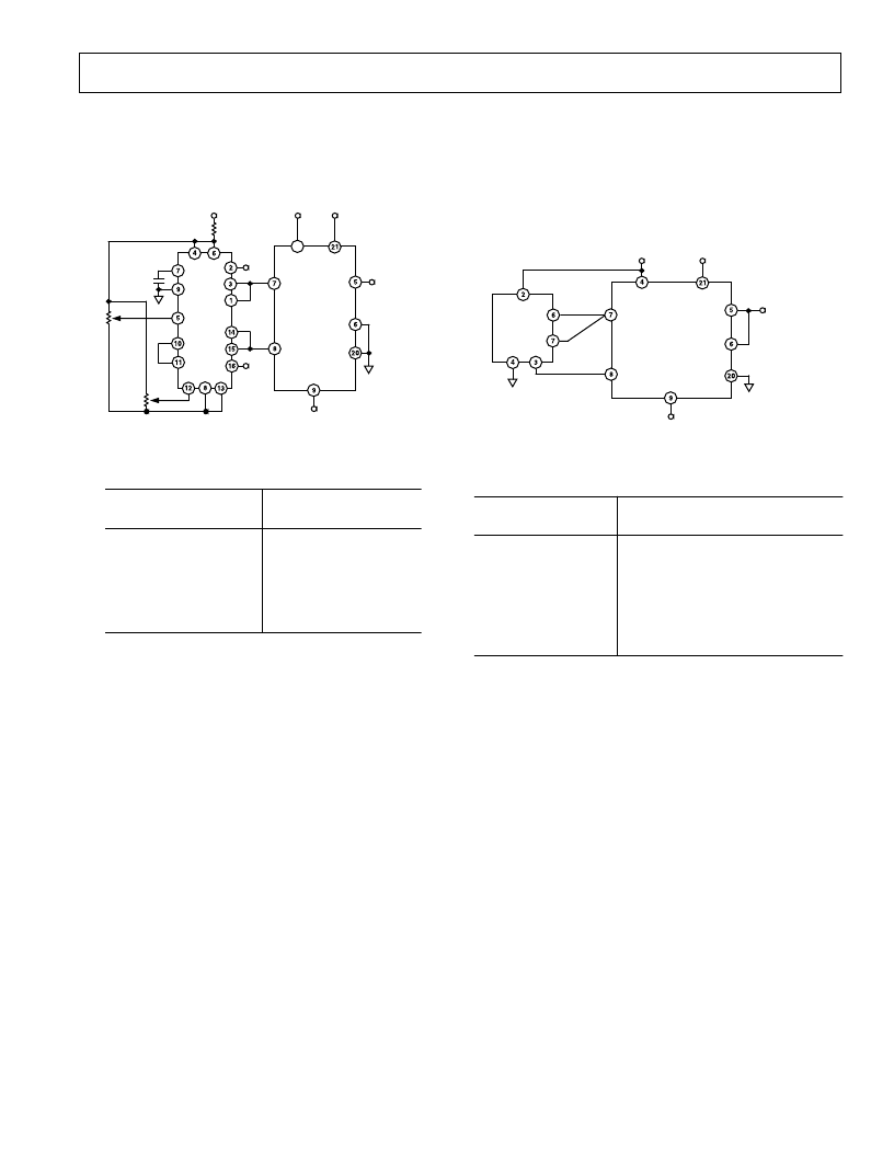
BIPOLAR OPERATION
Figure 19 shows the AD7846 set up for
±
10 V bipolar opera-
tion. The AD588 provides precision
±
5 V tracking outputs
which are fed to the V
REF+
and V
REF–
inputs of the AD7846.
The code table for Figure 19 is shown in Table IV.
R
IN
V
OUT
DGND
+15V
+5V
V
CC
V
DD
V
REF+
V
REF
–
R2
10k
C1
1 F
SIGNAL
GROUND
–
15V
*ADDITIONAL PINS
OMITTED FOR CLARITY
AD7846*
AD588
V
OUT
(
–
V
SS
+15V
–
15V
R3
100k
R1
+15V
4
Figure 19. Bipolar
±
10 V Operation
Table IV. Offset Binary Code Table for Figure 19
Binary Number
in DAC Latch
Analog Output
(V
OUT
)
MSB
1111 1111 1111 1111
1000 0000 0000 0001
1000 0000 0000 0000
0111 1111 1111 1111
0000 0000 0000 0000
LSB
+10 (32767/32768) V
+10 (1/32768) V
0 V
–10 (1/32768) V
–10 (32768/32768) V
NOTE
1 LSB = 10 V/2
15
= 10 V/32768 = 305
μ
V.
Full scale and bipolar zero adjustment are provided by varying
the gain and balance on the AD588. R2 varies the gain on the
AD588 while R3 adjusts the +5 V and –5 V outputs together
with respect to ground.
For bipolar zero adjustment on the AD7846, load the DAC with
100 . . . 000 and adjust R3 until V
OUT
= 0 V. Full scale is ad-
justed by loading the DAC with all 1s and adjusting R2 until
V
OUT
= 9.999694 V.
When bipolar zero and full scale adjustment are not needed, R2
and R3 can be omitted, Pin 12 on the AD588 should be con-
nected to Pin 11 and Pin 5 should be left floating. If a user
wants a +5 V output range, there are two choices. By tying Pin
6 (R
IN
) of the AD7846 to V
OUT
(Pin 5), the output stage gain is
reduced to unity and the output range is
±
5 V. If only a positive
+5 V reference is available, bipolar
±
5 V operation is still pos-
sible. Tie V
REF–
to 0 V and connect R
IN
to V
REF+
. This will also
give a
±
5 V output range. However, the linearity, gain, and
offset error specifications will be the same as the unipolar 0 V to
+5 V range.
Other Output Voltage Ranges
In some cases, users may require output voltage ranges other
than those already mentioned. One example is systems which
need the output voltage to be a whole number of millivolts (i.e.,
1 mV, 2 mV, etc.). If the AD689 (8.192 V reference) is used
with the AD7846 as in Figure 20, then the LSB size is 125
μ
V.
This makes it possible to program whole millivolt values at the
Output. Table V shows the code table for Figure 20.
R
IN
V
OUT
DGND
+15V
+5V
V
CC
V
DD
V
REF+
V
REF
–
SIGNAL GROUND
–
15V
*ADDITIONAL PINS
OMITTED FOR CLARITY
AD7846*
AD689
V
(0V TO 8.192V)
V
SS
Figure 20. Unipolar Output with AD689
Table V. Code Table for Figure 20
Binary Number
in DAC Latch
Analog Output
(V
OUT
)
MSB
1111 1111 1111 1111
1000 0000 0000 0000
0000 0000 0000 1000
0000 0000 0000 0100
0000 0000 0000 0010
0000 0000 0000 0001
LSB
8.192 V (65535/65536) = 8.1919 V
8.192 V (32768/65536) = 4.096 V
8.192 V (8/65536) = 0.001 V
8.192 V (4/65536) = 0.0005 V
8.192 V (2/65536) = 0.00025 V
8.192 V (1/65536) = 0.000125 V
NOTE
1 LSB = 8.192 V/2
l6
= 125
μ
V.
Multiplying Operation
The AD7846 is a full multiplying DAC. To get four-quadrant
multiplication, tie V
REF–
to 0 V, apply the ac input to V
REF+
and
tie R
IN
to V
REF+
. Figure 6 shows the Large Signal Frequency
Response when the DAC is used in this fashion.
相關PDF資料 |
PDF描述 |
|---|---|
| AD7846AP | LC2MOS 16-Bit Voltage Output DAC |
| AD7846AQ | LC2MOS 16-Bit Voltage Output DAC |
| AD7846BP | LC2MOS 16-Bit Voltage Output DAC |
| AD7846JN | LC2MOS 16-Bit Voltage Output DAC |
| AD7846JP | LC2MOS 16-Bit Voltage Output DAC |
相關代理商/技術參數 |
參數描述 |
|---|---|
| AD7846_10 | 制造商:AD 制造商全稱:Analog Devices 功能描述:LC2MOS 16-Bit Voltage Output DAC |
| AD7846ACHIPS | 制造商:AD 制造商全稱:Analog Devices 功能描述:LC2MOS 16-Bit Voltage Output DAC |
| AD7846AP | 功能描述:IC DAC 16BIT LC2MOS VOUT 28PLCC RoHS:否 類別:集成電路 (IC) >> 數據采集 - 數模轉換器 系列:- 產品培訓模塊:Lead (SnPb) Finish for COTS Obsolescence Mitigation Program 標準包裝:1,000 系列:- 設置時間:1µs 位數:8 數據接口:串行 轉換器數目:8 電壓電源:雙 ± 功率耗散(最大):941mW 工作溫度:0°C ~ 70°C 安裝類型:表面貼裝 封裝/外殼:24-SOIC(0.295",7.50mm 寬) 供應商設備封裝:24-SOIC W 包裝:帶卷 (TR) 輸出數目和類型:8 電壓,單極 采樣率(每秒):* |
| AD7846APZ | 功能描述:IC DAC 16BIT LC2MOS VOUT 28-PLCC RoHS:是 類別:集成電路 (IC) >> 數據采集 - 數模轉換器 系列:- 產品培訓模塊:Lead (SnPb) Finish for COTS Obsolescence Mitigation Program 標準包裝:1,000 系列:- 設置時間:1µs 位數:8 數據接口:串行 轉換器數目:8 電壓電源:雙 ± 功率耗散(最大):941mW 工作溫度:0°C ~ 70°C 安裝類型:表面貼裝 封裝/外殼:24-SOIC(0.295",7.50mm 寬) 供應商設備封裝:24-SOIC W 包裝:帶卷 (TR) 輸出數目和類型:8 電壓,單極 采樣率(每秒):* |
| AD7846AQ | 制造商:Rochester Electronics LLC 功能描述: 制造商:Analog Devices 功能描述:IC,D/A CONVERTER,SINGLE,16-BIT,BICMOS,DIP,28PIN |
發布緊急采購,3分鐘左右您將得到回復。