- 您現在的位置:買賣IC網 > PDF目錄373918 > AD7847BN (ANALOG DEVICES INC) LC2MOS Complete, Dual 12-Bit MDACs PDF資料下載
參數資料
| 型號: | AD7847BN |
| 廠商: | ANALOG DEVICES INC |
| 元件分類: | DAC |
| 英文描述: | LC2MOS Complete, Dual 12-Bit MDACs |
| 中文描述: | DUAL, PARALLEL, WORD INPUT LOADING, 3 us SETTLING TIME, 12-BIT DAC, PDIP24 |
| 封裝: | 0.300 INCH, PLASTIC, DIP-24 |
| 文件頁數: | 7/12頁 |
| 文件大小: | 187K |
| 代理商: | AD7847BN |
AD7837/AD7847
REV. C
–7–
CIRCUIT INFORMATION
D/A SECTION
A simplified circuit diagram for one of the D/A converters and
output amplifier is shown in Figure 10.
A segmented scheme is used whereby the 2 MSBs of the 12-bit
data word are decoded to drive the three switches A-C. The
remaining 10 bits drive the switches (S0–S9) in a standard R-2R
ladder configuration.
Each of the switches A–C steers 1/4 of the total reference cur-
rent with the remaining 1/4 passing through the R-2R section.
The output amplifier and feedback resistor perform the current
to voltage conversion giving
V
OUT
= –
D
×
V
REF
where
D
is the fractional representation of the digital word. (
D
can be set from 0 to 4095/4096.)
The output amplifier can maintain
±
10 V across a 2 k
load. It
is internally compensated and settles to 0.01% FSR (1/2 LSB)
in less than 5
μ
s. Note that on the AD7837, V
OUT
must be con-
nected externally to R
FB
.
V
OUT
R/2
R
V
REF
2R
2R
S0
AGND
R
2R
R
2R
2R
2R
2R
S8
S9
A
B
C
SHOWN FOR ALL 1s ON DAC
Figure 10. D/A Simplified Circuit Diagram
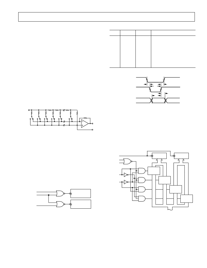
INTERFACE LOGIC INFORMATION—AD7847
The input control logic for the AD7847 is shown in Figure 11.
The part contains a 12-bit latch for each DAC. It can be treated
as two independent DACs, each with its own
CS
input and a com-
mon
WR
input.
CSA
and
WR
control the loading of data to the
DAC A latch, while
CSB
and
WR
control the loading of the
DAC B latch. The latches are edge triggered so that input data
is latched to the respective latch on the rising edge of
WR
. If
CSA
and
CSB
are both low and
WR
is taken high, the same data will
be latched to both DAC latches. The control logic truth table is
shown in Table I, while the write cycle timing diagram for the
part is shown in Figure 12.
CSA
WR
CSB
DAC A LATCH
DAC B LATCH
Figure 11. AD7847 Input Control Logic
Table I. AD7847 Truth Table
CSA
CSB
WR
Function
X
1
0
1
0
g
1
g
X
1
1
0
0
1
g
g
1
X
g
g
g
0
0
0
No Data Transfer
No Data Transfer
Data Latched to DAC A
Data Latched to DAC B
Data Latched to Both DACs
Data Latched to DAC A
Data Latched to DAC B
Data Latched to Both DACs
X = Don’t Care.
g
= Rising Edge Triggered.
DATA
t
1
t
2
t
3
t
5
t
4
CSA
,
CSB
WR
DATA
Figure 12. AD7847 Write Cycle Timing Diagram
INTERFACE LOGIC INFORMATION—AD7837
The input loading structure on the AD7837 is configured for
interfacing to microprocessors with an 8-bit-wide data bus. The
part contains two 12-bit latches per DAC—an input latch and
a DAC latch. Each input latch is further subdivided into a least-
significant 8-bit latch and a most-significant 4-bit latch. Only the
data held in the DAC latches determines the outputs from the part.
The input control logic for the AD7837 is shown in Figure 13,
while the write cycle timing diagram is shown in Figure 14.
DAC A MS
INPUT
LATCH
12
DAC A LS
INPUT
LATCH
4
8
DAC B LS
INPUT
LATCH
DAC B LS
INPUT
LATCH
12
4
8
8
CS
WR
DAC A
LATCH
LDAC
A0
A1
DB7 DB0
DAC B
LATCH
Figure 13. AD7837 Input Control Logic
相關PDF資料 |
PDF描述 |
|---|---|
| AD7847BQ | LC2MOS Complete, Dual 12-Bit MDACs |
| AD7847BR | LC2MOS Complete, Dual 12-Bit MDACs |
| AD7847SQ | LC2MOS Complete, Dual 12-Bit MDACs |
| AD7837AN | LC2MOS Complete, Dual 12-Bit MDACs |
| AD7837AQ | LC2MOS Complete, Dual 12-Bit MDACs |
相關代理商/技術參數 |
參數描述 |
|---|---|
| AD7847BN/883B | 制造商:AD 制造商全稱:Analog Devices 功能描述:LC2MOS Complete, Dual 12-Bit MDACs |
| AD7847BN883B | 制造商:AD 制造商全稱:Analog Devices 功能描述:LC2MOS Complete, Dual 12-Bit MDACs |
| AD7847BN-883B | 制造商:AD 制造商全稱:Analog Devices 功能描述:LC2MOS Complete, Dual 12-Bit MDACs |
| AD7847BNN | 制造商:AD 制造商全稱:Analog Devices 功能描述:LC2MOS Complete, Dual 12-Bit MDACs |
| AD7847BNQ | 制造商:AD 制造商全稱:Analog Devices 功能描述:LC2MOS Complete, Dual 12-Bit MDACs |
發布緊急采購,3分鐘左右您將得到回復。