- 您現(xiàn)在的位置:買賣IC網(wǎng) > PDF目錄373920 > AD7853BN (ANALOG DEVICES INC) 3 V to 5 V Single Supply, 200 kSPS 12-Bit Sampling ADCs PDF資料下載
參數(shù)資料
| 型號(hào): | AD7853BN |
| 廠商: | ANALOG DEVICES INC |
| 元件分類: | ADC |
| 英文描述: | 3 V to 5 V Single Supply, 200 kSPS 12-Bit Sampling ADCs |
| 中文描述: | 1-CH 12-BIT SUCCESSIVE APPROXIMATION ADC, SERIAL ACCESS, PDIP24 |
| 封裝: | 0.300 INCH, PLASTIC, DIP-24 |
| 文件頁數(shù): | 16/34頁 |
| 文件大小: | 350K |
| 代理商: | AD7853BN |
第1頁第2頁第3頁第4頁第5頁第6頁第7頁第8頁第9頁第10頁第11頁第12頁第13頁第14頁第15頁當(dāng)前第16頁第17頁第18頁第19頁第20頁第21頁第22頁第23頁第24頁第25頁第26頁第27頁第28頁第29頁第30頁第31頁第32頁第33頁第34頁
REV. B
–16–
AD7853/AD7853L
AIN(+)
AIN(–)
AMODE
AD7853/AD7853L
BIPOLAR
ANALOG
INPUT RANGE
SELECTED
Figure 15.
±
V
REF
/2 about V
REF
/2 Bipolar Input Configuration
DOUT
2S
COMPLEMENT
FORMAT
V
IN
= 0 TO V
REF
TRACK AND HOLD
AMPLIFIER
V
REF
/2
DV
DD
+FS –1LSB
OUTPUT
CODE
0V
111...111
111...110
111...101
111...100
000...011
000...001
000...000
000...010
V
IN
= (AIN(+) – AIN(–)), INPUT VOLTAGE
1LSB
1LSB =4096
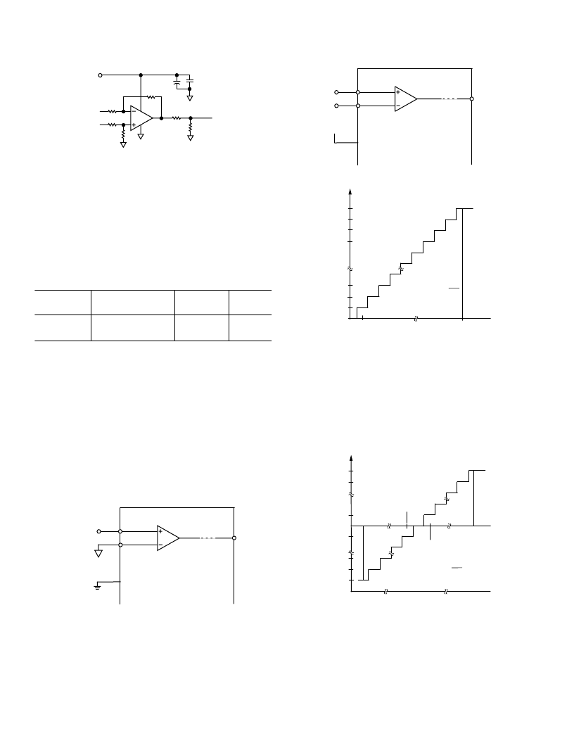
Figure 16. Unipolar Transfer Characteristic
Figure 15 shows the AD7853/AD7853L’s
±
V
REF
/2 bipolar ana-
log input configuration (where AIN(+) cannot go below 0 V so
for the full bipolar range then the AIN(–) pin should be biased
to +V
REF
/2). Once again the designed code transitions occur
midway between successive integer LSB values. The output
coding is twos complement with 1
LSB =
4096
=
3.3
V/
4096
=
0.8
mV
. The ideal input/output transfer characteristic is shown
in Figure 17.
– 1 LSB
FS = V
V
1LSB =4096
OUTPUT
CODE
011...111
V
REF
/2
011...110
000...001
000...000
100...001
100...000
100...010
V
IN
= (AIN(+) – AIN(–)), INPUT VOLTAGE
0V
+ FS
111...111
(V
REF
/2) –1 LSB
(V
REF
/2) +1 LSB
Figure 17. Bipolar Transfer Characteristic
IC1
AD820
AD820-3V
0.1
m
F
10
m
F
V+
V–
10k
V
50
V
10nF
(NPO)
TO AIN(+) OF
AD7853/AD7853L
V
IN
–V
REF
/2 TO +V
REF
/2
V
REF
/2
10k
V
10k
V
10k
V
+3V TO +5V
Figure 13. Analog Input Buffering
Input Ranges
The analog input range for the AD7853/AD7853L is 0 V to
V
REF
in both the unipolar and bipolar ranges.
The only difference between the unipolar range and the bipolar
range is that in the bipolar range the AIN(–) has to be biased up
to +V
REF
/2 and the output coding is twos complement (See
Table V and Figures 14 and 15). The unipolar or bipolar mode
is selected by the AMODE pin (0 for the unipolar range and 1
for the bipolar range).
Table V. Analog Input Connections
Analog Input
Range
0 V to V
REF1
±
V
REF
/2
2
Input Connections Connection
AIN(+)
AIN(–)
Diagram
AMODE
V
IN
V
IN
AGND
V
REF
/2
Figure 14
Figure 15
DGND
DV
DD
NOTES
1
Output code format is straight binary.
2
Range is
±
V
REF
/2 biased about V
REF
/2. Output code format is twos complement.
Note that the AIN(–) pin on the AD7853/AD7853L can be
biased up above AGND in the unipolar mode also, if required.
The advantage of biasing the lower end of the analog input
range away from AGND is that the user does not have to have
the analog input swing all the way down to AGND. This has the
advantage in true single supply applications that the input am-
plifier does not have to swing all the way down to AGND. The
upper end of the analog input range is shifted up by the same
amount. Care must be taken so that the bias applied does not
shift the upper end of the analog input above the AV
DD
supply.
In the case where the reference is the supply, AV
DD
, the AIN(–)
must be tied to AGND in unipolar mode.
AIN(+)
AIN(–)
AMODE
AD7853/AD7853L
UNIPOLAR ANALOG
INPUT RANGE
SELECTED
DOUT
STRAIGHT
BINARY
FORMAT
V
IN
= 0 TO V
REF
TRACK AND HOLD
AMPLIFIER
Figure 14. 0 to V
REF
Unipolar Input Configuration
Transfer Functions
For the unipolar range the designed code transitions occur
midway between successive integer LSB values (i.e., 1/2 LSB,
3/2 LSBs, 5/2 LSBs . . . FS –3/2 LSBs). The output coding is
straight binary for the unipolar range with 1
LSB = FS/
4096
=
3.3
V/
4096
=
0.8
mV
when
V
REF
= 3.3 V. The ideal input/output
transfer characteristic for the unipolar range is shown in
Figure 16.
相關(guān)PDF資料 |
PDF描述 |
|---|---|
| AD7853BR | 3 V to 5 V Single Supply, 200 kSPS 12-Bit Sampling ADCs |
| AD7853LAN | 3 V to 5 V Single Supply, 200 kSPS 12-Bit Sampling ADCs |
| AD7853LAR | 3 V to 5 V Single Supply, 200 kSPS 12-Bit Sampling ADCs |
| AD7853LBN | 3 V to 5 V Single Supply, 200 kSPS 12-Bit Sampling ADCs |
| AD7853LBR | 3 V to 5 V Single Supply, 200 kSPS 12-Bit Sampling ADCs |
相關(guān)代理商/技術(shù)參數(shù) |
參數(shù)描述 |
|---|---|
| AD7853BNZ | 功能描述:IC ADC 12BIT SRL 200KSPS 24-DIP RoHS:是 類別:集成電路 (IC) >> 數(shù)據(jù)采集 - 模數(shù)轉(zhuǎn)換器 系列:- 產(chǎn)品培訓(xùn)模塊:Lead (SnPb) Finish for COTS Obsolescence Mitigation Program 標(biāo)準(zhǔn)包裝:2,500 系列:- 位數(shù):12 采樣率(每秒):3M 數(shù)據(jù)接口:- 轉(zhuǎn)換器數(shù)目:- 功率耗散(最大):- 電壓電源:- 工作溫度:- 安裝類型:表面貼裝 封裝/外殼:SOT-23-6 供應(yīng)商設(shè)備封裝:SOT-23-6 包裝:帶卷 (TR) 輸入數(shù)目和類型:- |
| AD7853BR | 制造商:Analog Devices 功能描述:ADC Single SAR 200ksps 12-bit Serial 24-Pin SOIC W 制造商:Analog Devices 功能描述:Analog Devices AD7853BR Analog to Digital Converters (ADC) |
| AD7853BR-REEL | 制造商:Analog Devices 功能描述:ADC Single SAR 200ksps 12-bit Serial 24-Pin SOIC W T/R |
| AD7853BRZ | 功能描述:IC ADC 12BIT SRL 200KSPS 24SOIC RoHS:是 類別:集成電路 (IC) >> 數(shù)據(jù)采集 - 模數(shù)轉(zhuǎn)換器 系列:- 產(chǎn)品培訓(xùn)模塊:Lead (SnPb) Finish for COTS Obsolescence Mitigation Program 標(biāo)準(zhǔn)包裝:2,500 系列:- 位數(shù):12 采樣率(每秒):3M 數(shù)據(jù)接口:- 轉(zhuǎn)換器數(shù)目:- 功率耗散(最大):- 電壓電源:- 工作溫度:- 安裝類型:表面貼裝 封裝/外殼:SOT-23-6 供應(yīng)商設(shè)備封裝:SOT-23-6 包裝:帶卷 (TR) 輸入數(shù)目和類型:- |
| AD7853BRZ-REEL | 功能描述:IC ADC 12BIT SRL 200KSPS 24SOIC RoHS:是 類別:集成電路 (IC) >> 數(shù)據(jù)采集 - 模數(shù)轉(zhuǎn)換器 系列:- 標(biāo)準(zhǔn)包裝:1,000 系列:- 位數(shù):12 采樣率(每秒):300k 數(shù)據(jù)接口:并聯(lián) 轉(zhuǎn)換器數(shù)目:1 功率耗散(最大):75mW 電壓電源:單電源 工作溫度:0°C ~ 70°C 安裝類型:表面貼裝 封裝/外殼:24-SOIC(0.295",7.50mm 寬) 供應(yīng)商設(shè)備封裝:24-SOIC 包裝:帶卷 (TR) 輸入數(shù)目和類型:1 個(gè)單端,單極;1 個(gè)單端,雙極 |
發(fā)布緊急采購,3分鐘左右您將得到回復(fù)。