- 您現在的位置:買賣IC網 > PDF目錄373920 > AD7853L (Analog Devices, Inc.) 3 V to 5 V Single Supply, 200 kSPS 12-Bit Sampling ADCs(單電源,200kSPS 12位采樣A/D轉換器) PDF資料下載
參數資料
| 型號: | AD7853L |
| 廠商: | Analog Devices, Inc. |
| 英文描述: | 3 V to 5 V Single Supply, 200 kSPS 12-Bit Sampling ADCs(單電源,200kSPS 12位采樣A/D轉換器) |
| 中文描述: | 3 V至5 V單電源,200 kSPS的12位采樣ADC(單電源,速度高達200ksps的12位采樣的A / D轉換器) |
| 文件頁數: | 23/34頁 |
| 文件大小: | 350K |
| 代理商: | AD7853L |
第1頁第2頁第3頁第4頁第5頁第6頁第7頁第8頁第9頁第10頁第11頁第12頁第13頁第14頁第15頁第16頁第17頁第18頁第19頁第20頁第21頁第22頁當前第23頁第24頁第25頁第26頁第27頁第28頁第29頁第30頁第31頁第32頁第33頁第34頁
REV. B
–23–
AD7853/AD7853L
SERIAL INTERFACE SUMMARY
Table IX details the five interface modes and the serial clock
edges from which the data is clocked out by the AD7853/
AD7853L (DOUT Edge) and that the data is latched in on
(DIN Edge). The logic level of the POLARITY pin is shown
and it is clear that this reverses the edges.
In Interface Modes 4 and 5 the
SYNC
always clocks out the
first data bit and SCLK will clock out the subsequent bits.
In Interface Modes 1, 2, and 3 the
SYNC
is gated with the
SCLK and the POLARITY pin. Thus the
SYNC
may clock out
the MSB of data. Subsequent bits will be clocked out by the
serial clock, SCLK. The conditions for the
SYNC
clocking out
the MSB of data is as follows:
With the POLARITY pin high the falling edge of
SYNC
will clock
out the MSB if the serial clock is low when the
SYNC
goes low.
With the POLARITY pin low the falling edge of
SYNC
will clock
out the MSB if the serial clock is high when the
SYNC
goes low.
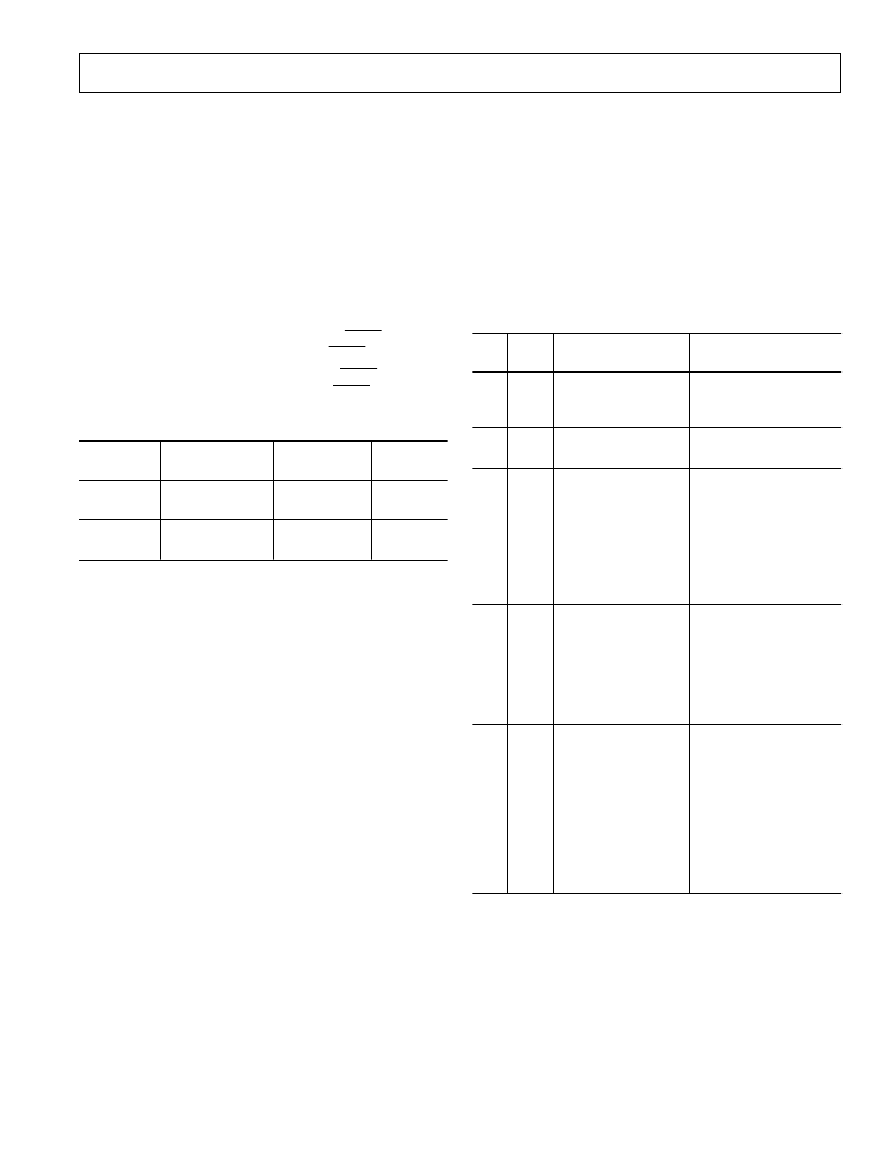
Table IX. SCLK Active Edge for Different Interface Modes
Interface
Mode
POLARITY
Pin
DOUT
Edge
SCLK
↑
SCLK
↓
SCLK
↓
SCLK
↑
DIN
Edge
SCLK
↓
SCLK
↑
SCLK
↑
SCLK
↓
1, 2, 3
0
1
4, 5
0
1
Resetting the Serial Interface
When writing to the part via the DIN line there is the possibility
of writing data into the incorrect registers, such as the test regis-
ter for instance, or writing the incorrect data and corrupting the
serial interface. The
SYNC
pin acts as a reset. Bringing the
SYNC
pin high resets the internal shift register. The first data
bit after the next
SYNC
falling edge will now be the first bit of a
new 16-bit transfer. It is also possible that the test register con-
tents were altered when the interface was lost. Therefore, once
the serial interface is reset, it may be necessary to write the 16-
bit word 0100 0000 0000 0010 to restore the test register to its
default value. Now the part and serial interface are completely
reset. It is always useful to retain the ability to program the
SYNC
line from a port of the
μ
Controller/DSP to have the
ability to reset the serial interface.
Table X summarizes the interface modes provided by the
AD7853/AD7853L. It also outlines the various
μ
P/
μ
C to which
the particular interface is suited.
The interface mode is determined by the serial mode selection
pins SM1 and SM2. Interface Mode 2 is the default mode. Note
that Interface Mode 1 and 2 have the same combination of SM1
and SM2. Interface Mode 1 may only be set by programming
the control register (see section on control register). External
SCLK and
SYNC
signals (
SYNC
may be hardwired low) are
required for Interfaces Modes 1, 2, and 3. In Interface Modes 4
and 5, the AD7853/AD7853L generates the SCLK and
SYNC
.
Some of the more popular
μ
Processors,
μ
Controllers, and the
DSP machines that the AD7853/AD7853L will interface to
directly are mentioned here. This does not cover all
μ
Cs,
μ
Ps
and DSPs. The interface mode of the AD7853/AD7853L that is
mentioned here for a specific
μ
C,
μ
P, or DSP is only a guide
and in most cases another interface mode may work just as well.
A more detailed timing description on each of the interface
modes follows.
Table X. Interface Mode Description
SM1
Pin
SM2
Pin
m
Processor/
m
Controller
Interface
Mode
0
0
8XC51
8XL51
PIC17C42
1 (2-Wire)
(DIN is an Input/
Output pin)
0
0
68HC11
68L11
2 (3-Wire, SPI/QSPI)
(Default Mode)
0
1
68HC16
PIC16C64
ADSP-21xx
DSP56000
DSP56001
DSP56002
DSP56L002
TMS320C30
3 (QSPI)
(External Serial
Clock, SCLK, and
External Frame Sync,
SYNC
, are required)
1
0
68HC16
4 (DSP is Slave)
(AD7853/AD7853L
generates a
noncontinuous
[16 clocks] Serial
Clock, SCLK, and the
Frame Sync,
SYNC
)
1
1
ADSP-21xx
DSP56000
DSP56001
DSP56002
DSP56L002
TMS320C20
TMS320C25
TMS320C30
TMS320C5x
TMS320LC5x
5 (DSP is Slave)
(AD7853/AD7853L
generates a
continuous Serial
Clock, SCLK, and the
Frame Sync,
SYNC
)
相關PDF資料 |
PDF描述 |
|---|---|
| AD7853 | 3 V to 5 V Single Supply, 200 KSPS 12-Bit Sampling ADCs(單電源,200kSPS 12位采樣A/D轉換器) |
| AD7853AN | 3 V to 5 V Single Supply, 200 kSPS 12-Bit Sampling ADCs |
| AD7853AR | 3 V to 5 V Single Supply, 200 kSPS 12-Bit Sampling ADCs |
| AD7853ARS | 3 V to 5 V Single Supply, 200 kSPS 12-Bit Sampling ADCs |
| AD7853BN | 3 V to 5 V Single Supply, 200 kSPS 12-Bit Sampling ADCs |
相關代理商/技術參數 |
參數描述 |
|---|---|
| AD7853LAN | 制造商:Analog Devices 功能描述:ADC Single SAR 100ksps 12-bit Serial 24-Pin PDIP 制造商:Analog Devices 功能描述:ADC SGL SAR 100KSPS 12-BIT SERL 24PDIP - Rail/Tube 制造商:Rochester Electronics LLC 功能描述:SELF CAL. SERIAL 12 BIT ADC I.C. - Bulk 制造商:Analog Devices 功能描述:IC 12BIT ADC 7853 DIP24 制造商:Analog Devices 功能描述:3 V to 5 V Single Supply, 200 kSPS 12-Bit Sampling ADCs |
| AD7853LANZ | 功能描述:IC ADC 12BIT SRL 200KSPS 24-DIP RoHS:是 類別:集成電路 (IC) >> 數據采集 - 模數轉換器 系列:- 標準包裝:1,000 系列:- 位數:12 采樣率(每秒):300k 數據接口:并聯 轉換器數目:1 功率耗散(最大):75mW 電壓電源:單電源 工作溫度:0°C ~ 70°C 安裝類型:表面貼裝 封裝/外殼:24-SOIC(0.295",7.50mm 寬) 供應商設備封裝:24-SOIC 包裝:帶卷 (TR) 輸入數目和類型:1 個單端,單極;1 個單端,雙極 |
| AD7853LAR | 功能描述:IC ADC 12BIT SRL 200KSPS 24-SOIC RoHS:否 類別:集成電路 (IC) >> 數據采集 - 模數轉換器 系列:- 標準包裝:1,000 系列:- 位數:12 采樣率(每秒):300k 數據接口:并聯 轉換器數目:1 功率耗散(最大):75mW 電壓電源:單電源 工作溫度:0°C ~ 70°C 安裝類型:表面貼裝 封裝/外殼:24-SOIC(0.295",7.50mm 寬) 供應商設備封裝:24-SOIC 包裝:帶卷 (TR) 輸入數目和類型:1 個單端,單極;1 個單端,雙極 |
| AD7853LAR-REEL | 功能描述:IC ADC 12BIT SRL 200KSPS 24-SOIC RoHS:否 類別:集成電路 (IC) >> 數據采集 - 模數轉換器 系列:- 產品培訓模塊:Lead (SnPb) Finish for COTS Obsolescence Mitigation Program 標準包裝:2,500 系列:- 位數:12 采樣率(每秒):3M 數據接口:- 轉換器數目:- 功率耗散(最大):- 電壓電源:- 工作溫度:- 安裝類型:表面貼裝 封裝/外殼:SOT-23-6 供應商設備封裝:SOT-23-6 包裝:帶卷 (TR) 輸入數目和類型:- |
發布緊急采購,3分鐘左右您將得到回復。