- 您現在的位置:買賣IC網 > PDF目錄373921 > AD7865YS-2 (ANALOG DEVICES INC) Four-Channel, Simultaneous Sampling, Fast, 14-Bit ADC PDF資料下載
參數資料
| 型號: | AD7865YS-2 |
| 廠商: | ANALOG DEVICES INC |
| 元件分類: | ADC |
| 英文描述: | Four-Channel, Simultaneous Sampling, Fast, 14-Bit ADC |
| 中文描述: | 4-CH 14-BIT SUCCESSIVE APPROXIMATION ADC, PARALLEL ACCESS, PQFP44 |
| 封裝: | PLASTIC, QFP-44 |
| 文件頁數: | 12/19頁 |
| 文件大小: | 195K |
| 代理商: | AD7865YS-2 |
AD7865
–12–
REV. A
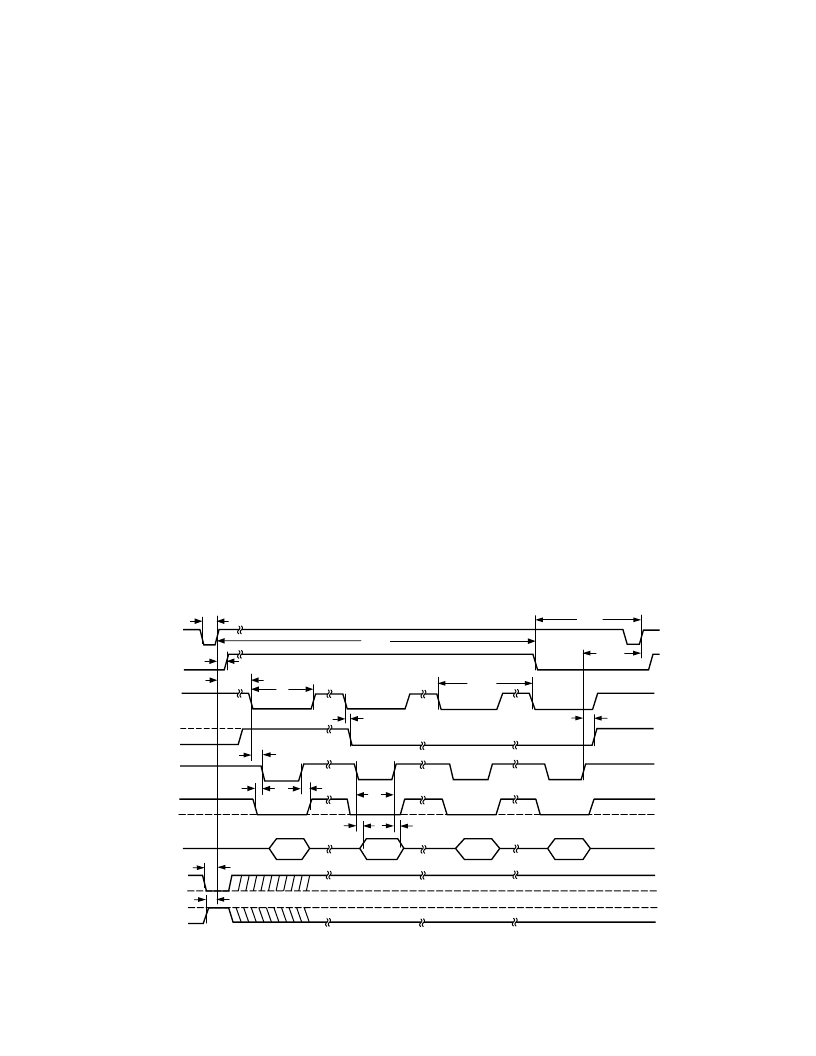
TIMING AND CONTROL
Reading Between Each Conversion in the Conversion Sequence
Figure 7 shows the timing and control sequence required to
obtain the optimum throughput rate from the AD7865. To
obtain the optimum throughput from the AD7865 the user must
read the result of each conversion as it becomes available. The
timing diagram in Figure 7 shows a read operation each time the
EOC
signal goes logic low. The timing in Figure 7 shows a
conversion on all four analog channels (SL1 to SL4 = 1, see
Selecting a Conversion Sequence), hence there are four
EOC
pulses and four read operations to access the result of each of
the four conversions.
A conversion is initiated on the rising edge of
CONVST
. This
places all four track/holds into hold simultaneously. New data
from this conversion sequence is available for the first channel
selected (A
IN1
) 2.4
μ
s later. The conversion on each subsequent
channel is completed at 2.4
μ
s intervals. The end of each con-
version is indicated by the falling edge of the
EOC
signal. The
BUSY output signal indicates the end of conversion for all se-
lected channels (four in this case).
Data is read from the part via a 14-bit parallel data bus with
standard
CS
and
RD
signals. The
CS
and
RD
inputs are inter-
nally gated to enable the conversion result onto the data bus.
The data lines DB0 to DB13 leave their high impedance state
when both
CS
and
RD
are logic low. Therefore,
CS
may be
permanently tied logic low and the
RD
signal used to access the
conversion result. Since each conversion result is latched into its
output data register at the same time
EOC
goes logic low a
further option would be to tie the
EOC
and
RD
pins together
with
CS
tied logic low and use the rising edge of
EOC
to latch
the conversion result. Although the AD7865 has some special
features that permit reading during a conversion (e.g., a sepa-
rate supply for the output data drivers, V
DRIVE
), for optimum
performance it is recommended that the read operation be
completed when
EOC
is logic low, i.e., before the start of the
next conversion. Although Figure 7 shows the read operation
taking place during the
EOC
pulse, a read operation can take
place at any time. Figure 7 shows a timing specification called
“Quiet Time.” This is the amount of time that should be left
after a read operation and before the next conversion is initi-
ated. The quiet time heavily depends on data bus capacitance
but a figure of 50 ns to 150 ns is typical.
The signal labeled FRSTDATA (First Data Word) indicates to
the user that the pointer associated with the output data regis-
ters is pointing to the first conversion result by going logic high.
The pointer is reset to point to the first data location (i.e., first
conversion result,) at the end of the first conversion just prior to
EOC
going low. The pointer is incremented to point to the next
register (next conversion result) by a rising edge of
RD
only if
that conversion result is available. If a read takes place before
the next conversion is complete (as shown in Figure 7) then the
pointer is incremented at the end of that conversion when the
EOC
pulse goes low. Hence, FRSTDATA in Figure 7 is seen to
go low just after to the second
EOC
pulse. Repeated read
operations during a conversion will continue to access the data
at the current pointer location until the pointer is incremented
at the end of that conversion. Note: FRSTDATA has an indeter-
minate logic state after initial power-up. This means that for the
first conversion sequence after power-up, the FRSTDATA
logic output may already be logic high before the end of the first
conversion. This condition is indicated by the dashed line in
Figure 8. Also the FRSTDATA logic output may already be
high as a result of the previous read sequence as is the case after
the fourth read in Figure 7. The forth read (rising edge of
RD
)
resets the pointer to the first data location. There, however,
FRSTDATA is already high when the next conversion sequence
is initiated.
QUIET
TIME
t
CONV
t
BUSY
t
1
t
12
t
3
t
4
t
5
t
6
t
7
V
IN1
V
IN2
V
IN3
V
IN4
100ns
100ns
DATA
CONVST
BUSY
EOC
FRSTDATA
RD
CS
H
/S SEL
SL1–SL4
t
2
t
ACQ
t
11
t
10
t
CONV
t
9
Figure 7. Timing Diagram for Reading During Conversion
相關PDF資料 |
PDF描述 |
|---|---|
| AD7865YS-3 | Four-Channel, Simultaneous Sampling, Fast, 14-Bit ADC |
| AD7865AS-1 | Four-Channel, Simultaneous Sampling, Fast, 14-Bit ADC |
| AD7865AS-2 | Four-Channel, Simultaneous Sampling, Fast, 14-Bit ADC |
| AD7865AS-3 | Four-Channel, Simultaneous Sampling, Fast, 14-Bit ADC |
| AD7865BS-1 | Four-Channel, Simultaneous Sampling, Fast, 14-Bit ADC |
相關代理商/技術參數 |
參數描述 |
|---|---|
| AD7865YS-3 | 制造商:Analog Devices 功能描述:ADC Single SAR 350ksps 14-bit Parallel 44-Pin MQFP |
| AD7865YS-3REEL | 制造商:Analog Devices 功能描述:ADC Single SAR 350ksps 14-bit Parallel 44-Pin MQFP T/R |
| AD7865YSZ-1 | 功能描述:IC ADC 14BIT 4CHAN 5V 44-MQFP RoHS:是 類別:集成電路 (IC) >> 數據采集 - 模數轉換器 系列:- 標準包裝:1 系列:- 位數:14 采樣率(每秒):83k 數據接口:串行,并聯 轉換器數目:1 功率耗散(最大):95mW 電壓電源:雙 ± 工作溫度:0°C ~ 70°C 安裝類型:通孔 封裝/外殼:28-DIP(0.600",15.24mm) 供應商設備封裝:28-PDIP 包裝:管件 輸入數目和類型:1 個單端,雙極 |
| AD7865YSZ-2 | 功能描述:IC ADC 14BIT 4CHAN 5V 44-MQFP RoHS:是 類別:集成電路 (IC) >> 數據采集 - 模數轉換器 系列:- 標準包裝:1 系列:- 位數:14 采樣率(每秒):83k 數據接口:串行,并聯 轉換器數目:1 功率耗散(最大):95mW 電壓電源:雙 ± 工作溫度:0°C ~ 70°C 安裝類型:通孔 封裝/外殼:28-DIP(0.600",15.24mm) 供應商設備封裝:28-PDIP 包裝:管件 輸入數目和類型:1 個單端,雙極 |
| AD7865YSZ-3 | 功能描述:IC ADC 14BIT 4CHAN 5V 44-MQFP RoHS:是 類別:集成電路 (IC) >> 數據采集 - 模數轉換器 系列:- 標準包裝:1 系列:- 位數:14 采樣率(每秒):83k 數據接口:串行,并聯 轉換器數目:1 功率耗散(最大):95mW 電壓電源:雙 ± 工作溫度:0°C ~ 70°C 安裝類型:通孔 封裝/外殼:28-DIP(0.600",15.24mm) 供應商設備封裝:28-PDIP 包裝:管件 輸入數目和類型:1 個單端,雙極 |
發布緊急采購,3分鐘左右您將得到回復。