- 您現在的位置:買賣IC網 > PDF目錄373921 > AD7870AQ (ANALOG DEVICES INC) LC2MOS Complete, 12-Bit, 100 kHz, Sampling ADCs PDF資料下載
參數資料
| 型號: | AD7870AQ |
| 廠商: | ANALOG DEVICES INC |
| 元件分類: | ADC |
| 英文描述: | LC2MOS Complete, 12-Bit, 100 kHz, Sampling ADCs |
| 中文描述: | 1-CH 12-BIT SUCCESSIVE APPROXIMATION ADC, SERIAL/PARALLEL ACCESS, CDIP24 |
| 封裝: | 0.300 INCH, HERMETIC SEALED, CERAMIC, DIP-24 |
| 文件頁數: | 4/20頁 |
| 文件大小: | 331K |
| 代理商: | AD7870AQ |
REV. B
AD7870/AD7875/AD7876
TIMNGCHARACTERISTICS
1, 2
–4–
Limit at T
, T
(J, K, L, A, B, C Versions)
Limit at T
, T
MAX
(S, T Versions)
Parameter
Units
Conditions/Comments
t
1
t
2
t
3
t
4
t
5
t
63
t
74
50
0
60
0
70
57
5
50
0
0
100
370
135
20
100
10
100
60
120
200
0
0
0
50
0
75
0
70
70
5
50
0
0
100
370
150
20
100
10
100
60
120
200
0
0
0
ns min
ns min
ns min
ns min
ns max
ns max
ns min
ns max
ns min
ns min
ns min
ns min
ns max
ns min
ns max
ns min
ns max
ns min
ns max
ns min
ns min
ns min
ns min
CONVST
Pulse Width
CS
to
RD
Setup T ime (Mode 1)
RD
Pulse Width
CS
to
RD
Hold T ime (Mode 1)
RD
to
INT
Delay
Data Access T ime after
RD
Bus Relinquish T ime after
RD
t
8
t
9
t
t
10
t
126
t
13
HBEN to
RD
Setup T ime
HBEN to
RD
Hold T ime
SSTRB
to SCLK Falling Edge Setup T ime
SCLK Cycle T ime
SCLK to Valid Data Delay. C
L
= 35 pF
SCLK Rising Edge to
SSTRB
t
14
Bus Relinquish T ime after SCLK
t
15
t
16
t
17
t
18
t
19
t
20
CS
to
RD
Setup T ime (Mode 2)
CS
to
BUSY
Propagation Delay
Data Setup T ime Prior to
BUSY
CS
to
RD
Hold T ime (Mode 2)
HBEN to
CS
Setup T ime
HBEN to
CS
Hold T ime
NOT ES
1
T iming specifications in
bold print
are 100% production tested. All other times are sample tested at +25
°
C to ensure compliance. All input signals are
specified with tr = tf = 5 ns (10% to 90% of 5 V) and timed from a voltage level of 1.6 V.
2
Serial timing is measured with a 4.7 k
pull-up resistor on SDAT A and
SSTRB
and a 2 k
pull-up on SCLK . T he capacitance on all three outputs is 35 pF.
3
t
6
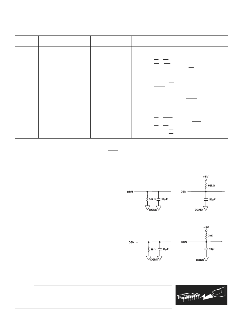
is measured with the load circuits of Figure 1 and defined as the time required for an output to cross 0.8 V or 2.4 V.
4
t
is defined as the time required for the data lines to change 0.5 V when loaded with the circuits of Figure 2.
5
SCLK mark/space ratio (measured from a voltage level of 1.6 V) is 40/60 to 60/40.
6
SDAT A will drive higher capacitive loads but this will add to t
12
since it increases the external RC time constant (4.7 k
i
C
L
) and hence the time to reach 2.4 V.
Specifications subject to chance without notice.
(V
DD
= +5 V
6
5%, V
SS
= –5 V
6
5%, AGND = DGND = 0 V. See Figures 9, 10, 11 and 12.)
ABSOLUT E MAX IMUM RAT INGS*
V
DD
to AGND . . . . . . . . . . . . . . . . . . . . . . . . . . –0.3 V to +7 V
V
SS
to AGND . . . . . . . . . . . . . . . . . . . . . . . . . . +0.3 V to –7 V
AGND to DGND . . . . . . . . . . . . . . . . . –0.3 V to V
DD
+0.3 V
V
IN
to AGND . . . . . . . . . . . . . . . . . . . . . . . . . –15 V to +15 V
REF OUT to AGND . . . . . . . . . . . . . . . . . . . . . . . . 0 V to V
DD
Digital Inputs to DGND . . . . . . . . . . . . –0.3 V to V
DD
+0.3 V
Digital Outputs to DGND . . . . . . . . . . . –0.3 V to V
DD
+0.3 V
Operating T emperature Range
Commercial (J, K , L Versions – AD7870) . . . 0
°
C to +70
°
C
Commercial (K , L Versions – AD7875) . . . . . 0
°
C to +70
°
C
Industrial (A, B, C Versions – AD7870) . . . .–25
°
C to +85
°
C
Industrial (B, C Versions – AD7875/AD7876)
. . . . . . . . . . . . . . . . . . . . . . . . . . . . . . . . . . .–40
°
C to +85
°
C
Extended (S, T Versions) . . . . . . . . . . . . . .–55
°
C to +125
°
C
Storage T emperature Range . . . . . . . . . . . . .–65
°
C to +150
°
C
Lead T emperature (Soldering, 10 sec) . . . . . . . . . . . . . +300
°
C
Power Dissipation (Any Package) to +75
°
C . . . . . . . . .450 mW
Derates above +75
°
C by . . . . . . . . . . . . . . . . . . . . . 10 mW/
°
C
*Stresses above those listed under “Absolute Maximum Ratings” may cause
permanent damage to the device. T his is a stress rating only; functional
operation of the device at these or any other conditions above those listed in
the operational sections of this specification is not implied. Exposure
to absolute maximum rating conditions for extended periods may affect
device reliability.
a. High-Z to V
OH
Figure 1. Load Circuits for Access Time
b. High-Z to V
OL
a. V
OH
to High-Z
b. V
OL
to High-Z
Figure 2. Load Circuits for Output Float Delay
CAUT ION
ESD (electrostatic discharge) sensitive device. Electrostatic charges as high as 4000 V readily
accumulate on the human body and test equipment and can discharge without detection. Although
the AD7870/AD7875/AD7876 feature proprietary ESD protection circuitry, permanent damage
may occur on devices subjected to high energy electrostatic discharges. T herefore, proper ESD
precautions are recommended to avoid performance degradation or loss of functionality.
WARNING!
ESD SENSITIVE DEVICE
相關PDF資料 |
PDF描述 |
|---|---|
| AD7870BQ | LC2MOS Complete, 12-Bit, 100 kHz, Sampling ADCs |
| AD7875BQ | LC2MOS Complete, 12-Bit, 100 kHz, Sampling ADCs |
| AD7875CQ | LC2MOS Complete, 12-Bit, 100 kHz, Sampling ADCs |
| AD7875KN | LC2MOS Complete, 12-Bit, 100 kHz, Sampling ADCs |
| AD7875KP | LC2MOS Complete, 12-Bit, 100 kHz, Sampling ADCs |
相關代理商/技術參數 |
參數描述 |
|---|---|
| AD7870BQ | 功能描述:IC ADC 12BIT SAMPLING 3V 24-CDIP RoHS:否 類別:集成電路 (IC) >> 數據采集 - 模數轉換器 系列:- 標準包裝:1 系列:- 位數:14 采樣率(每秒):83k 數據接口:串行,并聯 轉換器數目:1 功率耗散(最大):95mW 電壓電源:雙 ± 工作溫度:0°C ~ 70°C 安裝類型:通孔 封裝/外殼:28-DIP(0.600",15.24mm) 供應商設備封裝:28-PDIP 包裝:管件 輸入數目和類型:1 個單端,雙極 |
| AD7870CQ | 功能描述:IC ADC 12BIT SAMPLING 3V 24-CDIP RoHS:否 類別:集成電路 (IC) >> 數據采集 - 模數轉換器 系列:- 產品培訓模塊:Lead (SnPb) Finish for COTS Obsolescence Mitigation Program 標準包裝:250 系列:- 位數:12 采樣率(每秒):1.8M 數據接口:并聯 轉換器數目:1 功率耗散(最大):1.82W 電壓電源:模擬和數字 工作溫度:-40°C ~ 85°C 安裝類型:表面貼裝 封裝/外殼:48-LQFP 供應商設備封裝:48-LQFP(7x7) 包裝:管件 輸入數目和類型:2 個單端,單極 |
| AD7870JN | 功能描述:IC ADC 12BIT LC2MOS 100KHZ 24DIP RoHS:否 類別:集成電路 (IC) >> 數據采集 - 模數轉換器 系列:- 產品培訓模塊:Lead (SnPb) Finish for COTS Obsolescence Mitigation Program 標準包裝:2,500 系列:- 位數:12 采樣率(每秒):3M 數據接口:- 轉換器數目:- 功率耗散(最大):- 電壓電源:- 工作溫度:- 安裝類型:表面貼裝 封裝/外殼:SOT-23-6 供應商設備封裝:SOT-23-6 包裝:帶卷 (TR) 輸入數目和類型:- |
| AD7870JNZ | 功能描述:IC ADC 12BIT LC2MOS 100KHZ 24DIP RoHS:是 類別:集成電路 (IC) >> 數據采集 - 模數轉換器 系列:- 其它有關文件:TSA1204 View All Specifications 標準包裝:1 系列:- 位數:12 采樣率(每秒):20M 數據接口:并聯 轉換器數目:2 功率耗散(最大):155mW 電壓電源:模擬和數字 工作溫度:-40°C ~ 85°C 安裝類型:表面貼裝 封裝/外殼:48-TQFP 供應商設備封裝:48-TQFP(7x7) 包裝:Digi-Reel® 輸入數目和類型:4 個單端,單極;2 個差分,單極 產品目錄頁面:1156 (CN2011-ZH PDF) 其它名稱:497-5435-6 |
| AD7870JNZ1 | 制造商:AD 制造商全稱:Analog Devices 功能描述:LC2MOS Complete, 12-Bit, 100 kHz, Sampling ADCs |
發布緊急采購,3分鐘左右您將得到回復。