- 您現在的位置:買賣IC網 > PDF目錄373921 > AD7870JP (ANALOG DEVICES INC) LC2MOS Complete, 12-Bit, 100 kHz, Sampling ADCs PDF資料下載
參數資料
| 型號: | AD7870JP |
| 廠商: | ANALOG DEVICES INC |
| 元件分類: | ADC |
| 英文描述: | LC2MOS Complete, 12-Bit, 100 kHz, Sampling ADCs |
| 中文描述: | 1-CH 12-BIT SUCCESSIVE APPROXIMATION ADC, SERIAL/PARALLEL ACCESS, PQCC28 |
| 封裝: | PLASTIC, MO-047AB, LCC-28 |
| 文件頁數: | 15/20頁 |
| 文件大小: | 331K |
| 代理商: | AD7870JP |
REV. B
2
AD7870/AD7875/AD7876
–15–
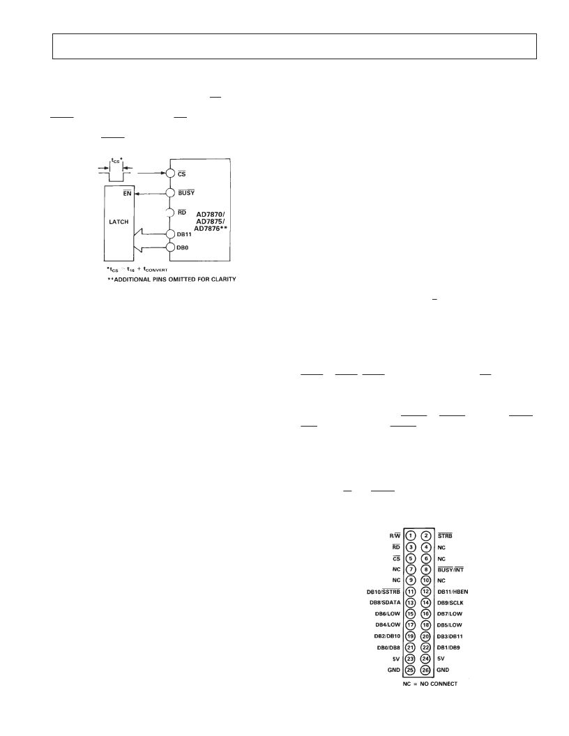
ST AND-ALONE OPE RAT ION
T he AD7870/AD7875/AD7876 can be used in its Mode 2, par-
allel interface mode for stand-alone operation. In this case, con-
version is initiated with a pulse to the ADC
CS
input. T his
pulse must be longer than the conversion time of the ADC. T he
BUSY
output is used to drive the
RD
input. Data is latched
from the ADC DB0–DB11 outputs to an external latch on the
rising edge of
BUSY
.
Figure 25. Stand-Alone Operation
APPLICAT ION HINT S
Good printed circuit board (PCB) layout is as important as the
overall circuit design itself in achieving high speed A/D perfor-
mance. T he designer has to be conscious of noise both in the
ADC itself and in the preceding analog circuitry. Switching
mode power supplies are not recommended as the switching
spikes will feed through to the comparator causing noisy code
transitions. Other causes of concern are ground loops and digi-
tal feedthrough from microprocessors. T hese are factors which
influence any ADC, and a proper PCB layout which minimizes
these effects is essential for best performance.
LAY OUT HINT S
Ensure that the layout for the printed circuit board has the digi-
tal and analog signal lines separated as much as possible. T ake
care not to run any digital track alongside an analog signal track.
Guard (screen) the analog input with AGND.
Establish a single point analog ground (star ground) separate
from the logic system ground at the AGND pin or as close as
possible to the ADC. Connect all other grounds and the
AD7870/AD7875/AD7876 DGND to this single analog ground
point. Do not connect any other digital grounds to this analog
ground point.
Low impedance analog and digital power supply common re-
turns are essential to low noise operation of the ADC, so make
the foil width for these tracks as wide as possible. T he use of
ground planes minimizes impedance paths and also guards the
analog circuitry from digital noise. T he circuit layout of Figures
30 and 31 have both analog and digital ground planes which are
kept separated and only joined together at the AD7870/
AD7875/AD7876 AGND pin.
NOISE
K eep the input signal leads to V
IN
and signal return leads from
AGND as short as possible to minimize input noise coupling. In
applications where this is not possible, use a shielded cable be-
tween the source and the ADC. Reduce the ground circuit im-
pedance as much as possible since any potential difference in
grounds between the signal source and the ADC appears as an
error voltage in series with the input signal.
DAT A ACQUISIT ION BOARD
Figure 28 shows the AD7870/AD7875/AD7876 in a data acqui-
sition circuit. T he corresponding printed circuit board (PCB)
layout and silkscreen are shown in Figures 29 to 31. T he board
layout has three interface ports: one serial and two parallel. One
of the parallel ports is directly compatible with the ADSP-2100
evaluation board expansion connector.
T he only additional component required for a full data acquisi-
tion system is an antialiasing filter. A component grid is pro-
vided near the analog input on the PCB, which may be used for
such a filter or any other input conditioning circuitry. T o facili-
tate this option there is a shorting plug (labelled LK 1 on the
PCB) on the analog input track. If this shorting plug is used, the
analog input connects to the buffer amplifier driving the ADC;
if this shorting plug is omitted, a wire link can be used to con-
nect the analog input to the PCB component grid.
INT E RFACE CONNE CT IONS
T here are two parallel connectors labeled SK T 4 and SK T 6 and
one serial connector labeled SK T 5. A shorting plug option
(LK 3 in Figure 28) on the ADC 12/
8
/CLK input configures
the ADC for the appropriate interface (see Pin Function
Description).
SK T 6 is a 96-contact (3-ROW) Eurocard connector that is
directly compatible with the ADSP-2100 Evaluation Board
Prototype Expansion Connector. T he expansion connector on
the ADSP-2100 has eight decoded chip enable outputs labeled
ECE1
to
ECE8
.
ECE6
is used to drive the ADC
CS
input on
the data acquisition board. T o avoid selecting on board RAM
sockets at the same time, LK 6 on the ADSP-2100 board must
be removed. In addition, the ADSP-2100 expansion connector
has four interrupts labelled
EIRQ0
to
EIRQ3
. T he ADC
BUSY
/
INT
output connects to
EIRQ0
. T here is a single wait state gen-
erator connected to EDMACK to allow the ADC to interface to
the faster versions of the ADSP-2100.
SK T 4 is a 26-way (2-ROW) IDC connector. T his connector
contains all the signal contacts as SK T 6 with the exception of
EDMACK which is connected to SK T 6 only. It also contains
decoded R/
W
and
STRB
inputs which are necessary for
T MS32020 interfacing. T he SK T 4 pinout is shown in Fig-
ure 26.
Figure 26. SKT4, IDC Connector Pinout
相關PDF資料 |
PDF描述 |
|---|---|
| AD7870KN | LC2MOS Complete, 12-Bit, 100 kHz, Sampling ADCs |
| AD7870KP | LC2MOS Complete, 12-Bit, 100 kHz, Sampling ADCs |
| AD7870LN | LC2MOS Complete, 12-Bit, 100 kHz, Sampling ADCs |
| AD7870LP | LC2MOS Complete, 12-Bit, 100 kHz, Sampling ADCs |
| AD7870SQ | LC2MOS Complete, 12-Bit, 100 kHz, Sampling ADCs |
相關代理商/技術參數 |
參數描述 |
|---|---|
| AD7870JP-REEL | 制造商:AD 制造商全稱:Analog Devices 功能描述:LC2MOS Complete, 12-Bit, 100 kHz, Sampling ADCs |
| AD7870JPZ | 功能描述:IC ADC 12BIT LC2MOS 28PLCC RoHS:是 類別:集成電路 (IC) >> 數據采集 - 模數轉換器 系列:- 其它有關文件:TSA1204 View All Specifications 標準包裝:1 系列:- 位數:12 采樣率(每秒):20M 數據接口:并聯 轉換器數目:2 功率耗散(最大):155mW 電壓電源:模擬和數字 工作溫度:-40°C ~ 85°C 安裝類型:表面貼裝 封裝/外殼:48-TQFP 供應商設備封裝:48-TQFP(7x7) 包裝:Digi-Reel® 輸入數目和類型:4 個單端,單極;2 個差分,單極 產品目錄頁面:1156 (CN2011-ZH PDF) 其它名稱:497-5435-6 |
| AD7870JPZ1 | 制造商:AD 制造商全稱:Analog Devices 功能描述:LC2MOS Complete, 12-Bit, 100 kHz, Sampling ADCs |
| AD7870JPZ-REEL | 功能描述:IC ADC 12BIT SAMPL LC2MOS 28PLCC RoHS:是 類別:集成電路 (IC) >> 數據采集 - 模數轉換器 系列:- 標準包裝:1 系列:- 位數:14 采樣率(每秒):83k 數據接口:串行,并聯 轉換器數目:1 功率耗散(最大):95mW 電壓電源:雙 ± 工作溫度:0°C ~ 70°C 安裝類型:通孔 封裝/外殼:28-DIP(0.600",15.24mm) 供應商設備封裝:28-PDIP 包裝:管件 輸入數目和類型:1 個單端,雙極 |
| AD7870JPZ-REEL1 | 制造商:AD 制造商全稱:Analog Devices 功能描述:LC2MOS Complete, 12-Bit, 100 kHz, Sampling ADCs |
發布緊急采購,3分鐘左右您將得到回復。