- 您現(xiàn)在的位置:買賣IC網(wǎng) > PDF目錄373921 > AD7870LN (ANALOG DEVICES INC) LC2MOS Complete, 12-Bit, 100 kHz, Sampling ADCs PDF資料下載
參數(shù)資料
| 型號: | AD7870LN |
| 廠商: | ANALOG DEVICES INC |
| 元件分類: | ADC |
| 英文描述: | LC2MOS Complete, 12-Bit, 100 kHz, Sampling ADCs |
| 中文描述: | 1-CH 12-BIT SUCCESSIVE APPROXIMATION ADC, SERIAL/PARALLEL ACCESS, PDIP24 |
| 封裝: | 0.300 INCH, PLASTIC, MS-001, DIP-24 |
| 文件頁數(shù): | 14/20頁 |
| 文件大小: | 331K |
| 代理商: | AD7870LN |
REV. B
AD7870/AD7875/AD7876
–14–
Serial Interfacing
Figures 21 to 24 show the AD7870/AD7875/AD7876 config-
ured for serial interfacing. In all four interfaces, the ADC is con-
figured for Mode 1 operation. T he interfaces show a timer
driving the
CONVST
input, but this could be generated from a
decoded address if required. T he SCLK , SDAT and
SSTRB
are
open-drain outputs. If these are required to drive capacitive
loads in excess 35 pF, buffering is recommended.
DSP56000 Serial Interface
Figure 21 shows a serial interface between the AD7870/
AD7875/AD7876 and the DSP56000. T he interface arrange-
ment is two-wire with the ADC configured for noncontinuous
clock operation (12/
8
/CLK = 0 V). T he DSP56000 is config-
ured for normal mode asynchronous operation with gated clock.
It is also set up for a 16-bit word with SCK and SC1 as inputs
and the FSL control bit set to a 0. In this configuration, the
DSP56000 assumes valid data on the first falling edge of SCK .
Since the ADC provides valid data on this first edge, there is no
need for a strobe or framing pulse for the data. SCLK and
SDAT A are gated off when the ADC is not performing a con-
version. During conversion, data is valid on the SDAT A output
of the ADC and is clocked into the receive data shift register of
the DSP56000. When this register has received 16 bits of data,
it generates an internal interrupt on the DSP56000 to read the
data from the register.
Figure 21. DSP56000 Serial Interface
T he DSP56000 and AD7870/AD7875/AD7876 can also be
configured for continuous clock operation (12/
8
/CLK = –5 V).
In this case, a strobe pulse is required by the DSP56000 to indi-
cate when data is valid. T he
SSTRB
output of the ADC is in-
verted and applied to the SC1 input of the DSP56000 to
provide this strobe pulse. All other conditions and connections
are the same as for gated clock operation.
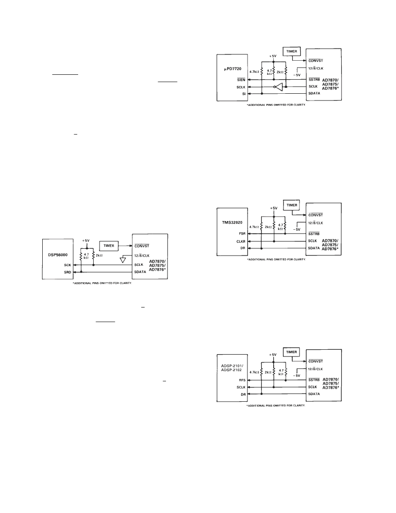
NEC7720/77230 Serial Interface
A serial interface between the AD7870/AD7875/AD7876 and
the NEC7720 is shown in Figure 22. In the interface shown, the
ADC is configured for continuous clock operation. T his can be
changed to a noncontinuous clock by simply tying the 12/
8
/CLK
input of the ADC to 0 V with all other connections remaining
the same. T he NEC7720 expects valid data on the rising edge of
its SCK input and therefore an inverter is required on the
SCLK output of the ADC. T he NEC7720 is configured for a
16-bit data word. Once the 16 bits of data have been received
by the SI register of the NEC7720, an internal interrupt is gen-
erated to read the contents of the SI register.
T he NEC77230 interface is similar to that just outlined for the
NEC7720. However, the clock input of the NEC77230 is
SICLK . Additionally, no inverter is required between the ADC
SCLK output and this SICLK input since the NEC77230 as-
sumes data is valid on the falling edge of SICLK .
Figure 22. NEC7720 Serial Interface
TMS32020 Serial Interface
Figure 23 shows a serial interface between the AD7870/ AD7875/
AD7876 and the T MS32020. T he AD7870/AD7875/AD7876 is
configured for continuous clock operation. Note, the ADC will
not interface correctly to the T MS32020 if the ADC is config-
ured for a noncontinuous clock. Data is clocked into the data
receive register (DRR) of the T MS32020 during conversion. As
with the previous interfaces, when a 16-bit word is received by
the T MS32020 it generates an internal interrupt to read the
data from the DRR.
Figure 23. TMS32020 Serial Interface
ADSP-2101/ADSP-2102 Serial Interface
Figure 24 shows a serial interface between the AD7870/AD7875/
AD7876 and the ADSP-2101/ADSP-2102. T he ADC is config-
ured for continuous clock operation. Data is clocked into the
serial port register of the ADSP-2101/ADSP-2102 during con-
version. As with the previous interfaces, when a 16-bit data
word is received by the ADSP-2101/ADSP-2102 an internal mi-
croprocessor interrupt is generated and the data is read from the
serial port register.
Figure 24. ADSP-2101/ADSP-2102 Serial Interface
相關(guān)PDF資料 |
PDF描述 |
|---|---|
| AD7870LP | LC2MOS Complete, 12-Bit, 100 kHz, Sampling ADCs |
| AD7870SQ | LC2MOS Complete, 12-Bit, 100 kHz, Sampling ADCs |
| AD7870TQ | LC2MOS Complete, 12-Bit, 100 kHz, Sampling ADCs |
| AD7876CN | 16-Bit, Pseudo Bipolar, Fully Diff Input, 250kSPS Serial Out, 2.7V to 5.5V Micro Power Sampling ADC 8-MSOP -40 to 85 |
| AD7876CQ | 16-Bit, Pseudo Bipolar, Fully Diff Input, 250kSPS Serial Out, 2.7V to 5.5V Micro Power Sampling ADC 8-MSOP -40 to 85 |
相關(guān)代理商/技術(shù)參數(shù) |
參數(shù)描述 |
|---|---|
| AD7870LNZ | 功能描述:IC ADC 12BIT SAMPLING 3V 24-DIP RoHS:是 類別:集成電路 (IC) >> 數(shù)據(jù)采集 - 模數(shù)轉(zhuǎn)換器 系列:- 標準包裝:1 系列:- 位數(shù):14 采樣率(每秒):83k 數(shù)據(jù)接口:串行,并聯(lián) 轉(zhuǎn)換器數(shù)目:1 功率耗散(最大):95mW 電壓電源:雙 ± 工作溫度:0°C ~ 70°C 安裝類型:通孔 封裝/外殼:28-DIP(0.600",15.24mm) 供應(yīng)商設(shè)備封裝:28-PDIP 包裝:管件 輸入數(shù)目和類型:1 個單端,雙極 |
| AD7870LNZ1 | 制造商:AD 制造商全稱:Analog Devices 功能描述:LC2MOS Complete, 12-Bit, 100 kHz, Sampling ADCs |
| AD7870LP | 制造商:AD 制造商全稱:Analog Devices 功能描述:LC2MOS Complete, 12-Bit, 100 kHz, Sampling ADCs |
| AD7870LP-REEL | 制造商:AD 制造商全稱:Analog Devices 功能描述:LC2MOS Complete, 12-Bit, 100 kHz, Sampling ADCs |
| AD7870LPZ | 功能描述:IC ADC 12BIT SAMPLING 3V 28-PLCC RoHS:是 類別:集成電路 (IC) >> 數(shù)據(jù)采集 - 模數(shù)轉(zhuǎn)換器 系列:- 標準包裝:1 系列:- 位數(shù):14 采樣率(每秒):83k 數(shù)據(jù)接口:串行,并聯(lián) 轉(zhuǎn)換器數(shù)目:1 功率耗散(最大):95mW 電壓電源:雙 ± 工作溫度:0°C ~ 70°C 安裝類型:通孔 封裝/外殼:28-DIP(0.600",15.24mm) 供應(yīng)商設(shè)備封裝:28-PDIP 包裝:管件 輸入數(shù)目和類型:1 個單端,雙極 |
發(fā)布緊急采購,3分鐘左右您將得到回復(fù)。