- 您現在的位置:買賣IC網 > PDF目錄373921 > AD7870TQ (ANALOG DEVICES INC) LC2MOS Complete, 12-Bit, 100 kHz, Sampling ADCs PDF資料下載
參數資料
| 型號: | AD7870TQ |
| 廠商: | ANALOG DEVICES INC |
| 元件分類: | ADC |
| 英文描述: | LC2MOS Complete, 12-Bit, 100 kHz, Sampling ADCs |
| 中文描述: | 1-CH 12-BIT SUCCESSIVE APPROXIMATION ADC, SERIAL/PARALLEL ACCESS, CDIP24 |
| 封裝: | 0.300 INCH, HERMETIC SEALED, CERAMIC, DIP-24 |
| 文件頁數: | 6/20頁 |
| 文件大小: | 331K |
| 代理商: | AD7870TQ |
REV. B
AD7870/AD7875/AD7876
–6–
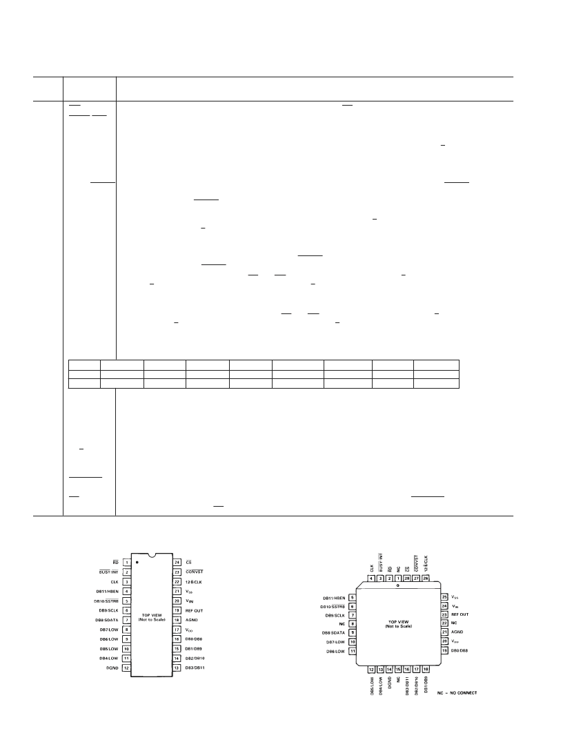
PIN FUNCT ION DE SCRIPT ION
DIP
Pin No.
Pin
Mnemonic
Function
1
2
3
RD
BUSY
/
INT
CLK
Read. Active low logic input. T his input is used in conjunction with
CS
low to enable the data outputs.
Busy/Interrupt, Active low logic output indicating converter status. See timing diagrams.
Clock input. An external T T L-compatible clock may be applied to this input pin. Alternatively, tying this pin to
V
SS
enables the internal laser-trimmed clock oscillator.
Data Bit 11 (MSB)/High Byte Enable. T he function of this pin is dependent on the state of the 12/
8
/CLK input (see
below). When 12-bit parallel data is selected, this pin provides the DB11 output. When byte data is selected, this pin
becomes the HBEN logic input HBEN is used for 8-bit bus interfacing. When HBEN is low, DB7/LOW to DB0/DB8
become DB7 to DB0. With HBEN high, DB7/LOW to DB0/DB8 are used for the upper byte of data (see T able I).
DB10/
SSTRB
Data Bit 10/Serial Strobe. When 12-bit parallel data is selected, this pin provides the DB10 output.
SSTRB
is an
active low open-drain output that provides a strobe or framing pulse for serial data. An external 4.7 k
pull-up
resistor is required on
SSTRB
.
DB9/SCLK
Data Bit 9/Serial Clock. When 12-bit parallel data is selected, this pin provides the DB9 output. SCLK is the gated
serial clock output derived from the internal or external ADC clock. If the 12/
8
/CLK input is at –5 V, then SCLK
runs continuously. If 12/
8
/CLK is at 0 V, then SCLK is gated off after serial transmission is complete. SCLK is an
open-drain output and requires an external 2 k
pull-up resistor.
DB8/SDAT A
Data Bit 8/Serial Data. When 12-bit parallel data is selected, this pin provides the DB8 output. SDAT A is an open-
drain serial data output which is used with SCLK and
SSTRB
for serial data transfer. Serial data is valid on the fall-
ing edge of SCLK while
SSTRB
is low. An external 4.7 k
pull-up resistor is required on SDAT A.
DB7/LOW–
T hree-state data outputs controlled by
CS
and
RD
. T heir function depends on the 12/
8
/CLK and HBEN inputs.
DB4/LOW
With 12/
8
/CLK high, they are always DB7–DB4. With 12/
8
/CLK low or –5 V, their function is controlled by HBEN
(see T able I).
DGND
Digital Ground. Ground reference for digital circuitry.
DB3/DB11–
T hree-state data outputs which are controlled by
CS
and
RD
. T heir function depends on the 12/
8
/CLK and HBEN
DB0/DB8
inputs. With 12/
8
/CLK high, they are always DB3–DB0. With 12/
8
/CLK low or –5 V, their function is controlled by
HBEN (see T able I).
4
DB11/HBEN
5
6
7
8–11
12
13–16
T able I. Output Data for Byte Interfacing
HBEN
HIGH
LOW
DB7/LOW DB6/LOW
LOW
DB7
DB5/LOW DB4/LOW
LOW
DB5
DB3/DB11
DB11(MSB)
DB3
DB2/DB10
DB10
DB2
DB1/DB9
DB9
DB1
DB0/DB8
DB8
DB0 (LSB)
LOW
DB6
LOW
DB4
17
18
19
20
21
22
V
DD
AGND
REF OUT
V
IN
V
SS
12/
8
/CLK
Positive Supply, +5 V
±
5%.
Analog Ground. Ground reference for track/hold, reference and DAC.
Voltage Reference Output. T he internal 3 V reference is provided at this pin. T he external load capability is 500
μ
A.
Analog Input. T he analog input range is
±
3 V for the AD7870,
±
10 V for the AD7876 and 0 V to +5 V for the AD7875.
Negative Supply, –5 V
±
5%.
T hree Function Input. Defines the data format and serial clock format. With this pin at +5 V, the output data for-
mat is 12-bit parallel only. With this pin at 0 V, either byte or serial data is available and SCLK is not continuous.
With this pin at –5 V, either byte or serial data is again available but SCLK is now continuous.
Convert Start. A low to high transition on this input puts the track/hold into its hold mode and starts conversion.
T his input is asynchronous to the CLK input.
Chip Select. Active low logic input. T he device is selected when this input is active. With
CONVST
tied low, a new
conversion is initiated when
CS
goes low.
23
CONVST
24
CS
DIP and SOIC
2
PLC C
2
PIN CONFIGURAT IONS
1
1
PIN CONFIGURATIONS ARE THE SAME FOR
THE AD7875 AND AD7876.
2
THE AD7870 AND AD7875 ARE AVAILABLE IN
DIP AND PLCC; THE AD7870A IS AVAILABLE IN
PLASTIC DIP; THE AD7875 AND AD7876 ARE
AVAILABLE IN SOIC AND DIP.
相關PDF資料 |
PDF描述 |
|---|---|
| AD7876CN | 16-Bit, Pseudo Bipolar, Fully Diff Input, 250kSPS Serial Out, 2.7V to 5.5V Micro Power Sampling ADC 8-MSOP -40 to 85 |
| AD7876CQ | 16-Bit, Pseudo Bipolar, Fully Diff Input, 250kSPS Serial Out, 2.7V to 5.5V Micro Power Sampling ADC 8-MSOP -40 to 85 |
| AD7876CR | 16-Bit, Pseudo Bipolar, Fully Diff Input, 250kSPS Serial Out, 2.7V to 5.5V Micro Power Sampling ADC 8-MSOP -40 to 85 |
| AD7876TQ | 16-Bit, Pseudo Bipolar, Fully Diff Input, 250kSPS Serial Out, 2.7V to 5.5V Micro Power Sampling ADC 8-MSOP -40 to 85 |
| AD7870AQ | LC2MOS Complete, 12-Bit, 100 kHz, Sampling ADCs |
相關代理商/技術參數 |
參數描述 |
|---|---|
| AD7870TQ/883B | 制造商:未知廠家 制造商全稱:未知廠家 功能描述:Analog-to-Digital Converter, 12-Bit |
| AD7871 | 制造商:AD 制造商全稱:Analog Devices 功能描述:LC2MOS Complete 14-Bit, Sampling ADCs |
| AD7871AQ | 制造商:未知廠家 制造商全稱:未知廠家 功能描述:Analog-to-Digital Converter, 14-Bit |
| AD7871BQ | 制造商:未知廠家 制造商全稱:未知廠家 功能描述:Analog-to-Digital Converter, 14-Bit |
| AD7871JN | 功能描述:IC ADC 14BIT SAMPLING 28-DIP RoHS:否 類別:集成電路 (IC) >> 數據采集 - 模數轉換器 系列:- 標準包裝:1 系列:- 位數:14 采樣率(每秒):83k 數據接口:串行,并聯 轉換器數目:1 功率耗散(最大):95mW 電壓電源:雙 ± 工作溫度:0°C ~ 70°C 安裝類型:通孔 封裝/外殼:28-DIP(0.600",15.24mm) 供應商設備封裝:28-PDIP 包裝:管件 輸入數目和類型:1 個單端,雙極 |
發布緊急采購,3分鐘左右您將得到回復。