- 您現在的位置:買賣IC網 > PDF目錄373922 > AD7874 (Analog Devices, Inc.) 4-Channel, 12-Bit Simultaneous Sampling Data Acquisition System(LC2MOS 4通道,12位同時采樣DAS) PDF資料下載
參數資料
| 型號: | AD7874 |
| 廠商: | Analog Devices, Inc. |
| 英文描述: | 4-Channel, 12-Bit Simultaneous Sampling Data Acquisition System(LC2MOS 4通道,12位同時采樣DAS) |
| 中文描述: | 4通道,12位同時采樣數據采集系統(LC2MOS 4通道,12位同時采樣DAS)的 |
| 文件頁數: | 3/16頁 |
| 文件大小: | 427K |
| 代理商: | AD7874 |
AD7874
REV. C
–3–
TIMNGCHARACTERISTICS
1
Parameter
A, B Versions
S Version
Units
Conditions/Comments
t
1
t
2
t
3
t
4
t
5
t
62
t
73
50
0
60
0
60
57
5
45
130
31
32.5
31
35
10
50
0
70
0
60
70
5
50
150
31
32.5
31
35
10
ns min
ns min
ns min
ns min
ns max
ns max
ns min
ns max
ns min
μ
s min
μ
s max
μ
s min
μ
s max
μ
s max
CONVST
Pulse Width
CS
to
RD
Setup T ime
RD
Pulse Width
CS
to
RD
Hold T ime
RD
to
INT
Delay
Data Access T ime after
RD
Bus Relinquish T ime after
RD
t
8
t
CONV
Delay T ime between Reads
CONVST
to
INT
, External Clock
CONVST
to
INT
, External Clock
CONVST
to
INT
, Internal Clock
CONVST
to
INT
, Internal Clock
Minimum Input Clock Period
t
CLK
NOT ES
1
T iming Specifications in
bold print
are 100% production tested. All other times are sample tested at +25
°
C to ensure compliance. All input signals are specified with
tr = tf = 5 ns (10% to 90% of +5 V) and timed from a voltage level of 1.6 V.
2
t
6
is measured with the load circuit of Figure 1 and defined as the time required for an output to cross 0.8 V or 2.4 V.
3
t
is derived from the measured time taken by the data outputs to change 0.5 V when loaded with the circuit of Figure 2. T he measured number is then extrapolated
back to remove the effects of charging or discharging the 50 pF capacitor. T his means that the time, t
7
, quoted in the timing characteristics is the true bus relinquish
time of the part and as such is independent of external bus loading capacitances.
Specifications subject to change without notice.
(V
DD
= +5 V
6
5%, V
SS
= –5 V
6
5%, AGND = DGND = OV, t
CLK
= 2.5 MHz external unless
otherwse noted.)
ABSOLUT E MAX IMUM RAT INGS*
(T
A
= +25
°
C unless otherwise noted)
V
DD
to AGND . . . . . . . . . . . . . . . . . . . . . . . . . –0.3 V to +7 V
V
DD
to DGND . . . . . . . . . . . . . . . . . . . . . . . . . –0.3 V to +7 V
V
SS
to AGND . . . . . . . . . . . . . . . . . . . . . . . . . +0.3 V to –7 V
AGND to DGND . . . . . . . . . . . . . . . . –0.3 V to V
DD
+ 0.3 V
V
IN
to AGND . . . . . . . . . . . . . . . . . . . . . . . . .–15 V to +15 V
REF OUT to AGND . . . . . . . . . . . . . . . . . . . . . . . 0 V to V
DD
Digital Inputs to DGND . . . . . . . . . . . –0.3 V to V
DD
+ 0.3 V
Digital Outputs to DGND . . . . . . . . . . –0.3 V to V
DD
+ 0.3 V
Operating T emperature Range
Commercial (A, B Versions) . . . . . . . . . . . –40
°
C to +85
°
C
Extended (S Version) . . . . . . . . . . . . . . . . –55
°
C to +125
°
C
Storage T emperature Range . . . . . . . . . . . . –65
°
C to +150
°
C
Lead T emperature (Soldering, 10 secs) . . . . . . . . . . . +300
°
C
Power Dissipation (Any Package) to +75
°
C . . . . . . 1,000 mW
Derates above +75
°
C by . . . . . . . . . . . . . . . . . . . . 10 mW/
°
C
*Stresses above those listed under “Absolute Maximum Ratings” may cause
permanent damage to the device. T his is a stress rating only and functional
operation of the device at these or any other conditions above those listed in the
operational sections of this specifications is not implied. Exposure to absolute
maximum rating conditions for extended periods may affect device reliability.
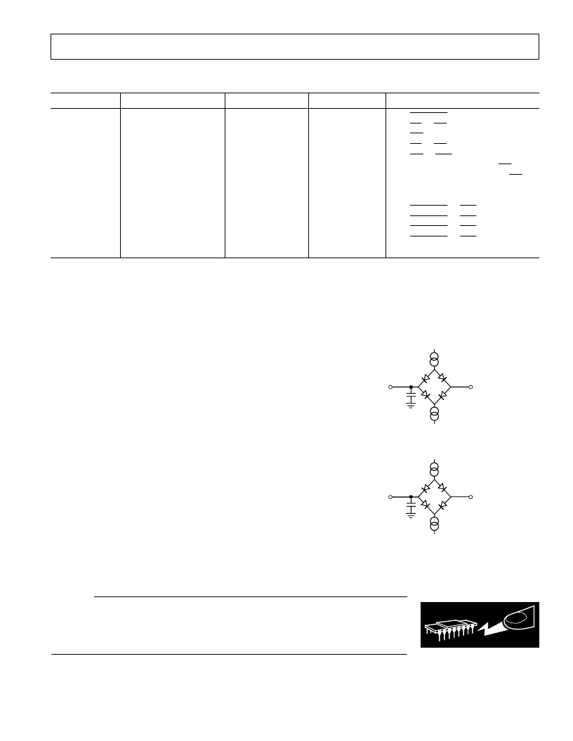
TO OUTPUT
PIN
1.6mA
2.1V
+
200
μ
A
50pF
Figure 1. Load Circuit for Access Time
TO OUTPUT
PIN
1.6mA
2.1V
+
200
μ
A
50pF
Figure 2. Load Circuit for Bus Relinquish Time
WARNING!
ESD SENSITIVE DEVICE
C AUT ION
ESD (electrostatic discharge) sensitive device. Electrostatic charges as high as 4000 V readily
accumulate on the human body and test equipment and can discharge without detection.
Although the AD7874 features proprietary ESD protection circuitry, permanent damage may
occur on devices subjected to high energy electrostatic discharges. T herefore, proper ESD
precautions are recommended to avoid performance degradation or loss of functionality.
相關PDF資料 |
PDF描述 |
|---|---|
| AD7878SQ | IC 1:10 CLOCK DRIVER 20-QSOP |
| AD7878 | LC2MOS Complete 12-Bit 100 kHz Sampling ADC with DSP Interface |
| AD7878AQ | LC2MOS Complete 12-Bit 100 kHz Sampling ADC with DSP Interface |
| AD7878BQ | LC2MOS Complete 12-Bit 100 kHz Sampling ADC with DSP Interface |
| AD7878KN | LC2MOS Complete 12-Bit 100 kHz Sampling ADC with DSP Interface |
相關代理商/技術參數 |
參數描述 |
|---|---|
| AD7874AN | 功能描述:IC DAS 12BIT 4CH LC2MOS 28-DIP RoHS:否 類別:集成電路 (IC) >> 數據采集 - ADCs/DAC - 專用型 系列:- 產品培訓模塊:Lead (SnPb) Finish for COTS Obsolescence Mitigation Program 標準包裝:50 系列:- 類型:數據采集系統(DAS) 分辨率(位):16 b 采樣率(每秒):21.94k 數據接口:MICROWIRE?,QSPI?,串行,SPI? 電壓電源:模擬和數字 電源電壓:1.8 V ~ 3.6 V 工作溫度:-40°C ~ 85°C 安裝類型:表面貼裝 封裝/外殼:40-WFQFN 裸露焊盤 供應商設備封裝:40-TQFN-EP(6x6) 包裝:托盤 |
| AD7874ANZ | 功能描述:IC DAS 12BIT 4CH LC2MOS 28-DIP RoHS:是 類別:集成電路 (IC) >> 數據采集 - ADCs/DAC - 專用型 系列:- 產品培訓模塊:Data Converter Basics 標準包裝:1 系列:- 類型:電機控制 分辨率(位):12 b 采樣率(每秒):1M 數據接口:串行,并聯 電壓電源:單電源 電源電壓:2.7 V ~ 3.6 V,4.5 V ~ 5.5 V 工作溫度:-40°C ~ 85°C 安裝類型:表面貼裝 封裝/外殼:100-TQFP 供應商設備封裝:100-TQFP(14x14) 包裝:剪切帶 (CT) 其它名稱:296-18373-1 |
| AD7874ANZ | 制造商:Analog Devices 功能描述:IC 12-BIT ADC |
| AD7874AQ | 功能描述:IC DAS 12BIT 4CH 5V 28-CDIP RoHS:否 類別:集成電路 (IC) >> 數據采集 - ADCs/DAC - 專用型 系列:- 產品培訓模塊:Lead (SnPb) Finish for COTS Obsolescence Mitigation Program 標準包裝:50 系列:- 類型:數據采集系統(DAS) 分辨率(位):16 b 采樣率(每秒):21.94k 數據接口:MICROWIRE?,QSPI?,串行,SPI? 電壓電源:模擬和數字 電源電壓:1.8 V ~ 3.6 V 工作溫度:-40°C ~ 85°C 安裝類型:表面貼裝 封裝/外殼:40-WFQFN 裸露焊盤 供應商設備封裝:40-TQFN-EP(6x6) 包裝:托盤 |
| AD7874AR | 功能描述:IC DAS 12BIT 4CH LC2MOS 28-SOIC RoHS:否 類別:集成電路 (IC) >> 數據采集 - ADCs/DAC - 專用型 系列:- 產品培訓模塊:Lead (SnPb) Finish for COTS Obsolescence Mitigation Program 標準包裝:50 系列:- 類型:數據采集系統(DAS) 分辨率(位):16 b 采樣率(每秒):21.94k 數據接口:MICROWIRE?,QSPI?,串行,SPI? 電壓電源:模擬和數字 電源電壓:1.8 V ~ 3.6 V 工作溫度:-40°C ~ 85°C 安裝類型:表面貼裝 封裝/外殼:40-WFQFN 裸露焊盤 供應商設備封裝:40-TQFN-EP(6x6) 包裝:托盤 |
發布緊急采購,3分鐘左右您將得到回復。