- 您現(xiàn)在的位置:買賣IC網(wǎng) > PDF目錄373922 > AD7875TQ (ANALOG DEVICES INC) LC2MOS Complete, 12-Bit, 100 kHz, Sampling ADCs PDF資料下載
參數(shù)資料
| 型號: | AD7875TQ |
| 廠商: | ANALOG DEVICES INC |
| 元件分類: | ADC |
| 英文描述: | LC2MOS Complete, 12-Bit, 100 kHz, Sampling ADCs |
| 中文描述: | 1-CH 12-BIT SUCCESSIVE APPROXIMATION ADC, SERIAL/PARALLEL ACCESS, CDIP24 |
| 封裝: | 0.300 INCH, HERMETIC SEALED, CERAMIC, DIP-24 |
| 文件頁數(shù): | 7/20頁 |
| 文件大小: | 331K |
| 代理商: | AD7875TQ |
REV. B
2
AD7870/AD7875/AD7876
–7–
to the conversion time plus the track/hold amplifier
acquisition time. For a 2.5 MHz input clock the throughput
rate is 10
μ
s max.
T he operation of the track/hold is essentially transparent to the
user. T he track/hold amplifier goes from its tracking mode to its
hold mode at the start of conversion. If the
CONVST
input is
used to start conversion then the track to hold transition occurs
on the rising edge of
CONVST
. If
CS
starts conversion, this
transition occurs on the falling edge of
CS
.
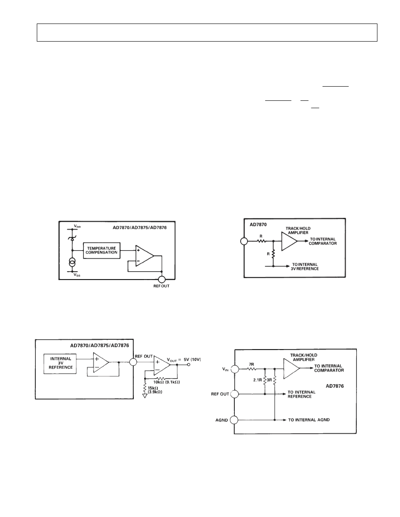
ANALOG INPUT
T he three parts differ from each other in the analog input volt-
age range that they can handle. T he AD7870 accepts
±
3 V
input signals, the AD7876 accepts a
±
10 V input range, while
the input range for the AD7875 is 0 V to +5 V.
Figure 5a shows the AD7870 analog input. T he analog input
range is
±
3 V into an input resistance of typically 15 k
. T he
designed code transitions occur midway between successive
integer LSB values (i.e., 1/2 LSB, 3/2 LSBs, 5/2 LSBs . . .
FS–3/2 LSBs). T he output code is twos complement binary
with 1 LSB = FS/4096 = 6 V/4096 = 1.46 mV. T he ideal input/
output transfer function is shown in Figure 6.
Figure 5a. AD7870 Analog Input
T he AD7876 analog input structure is shown in Figure 5b. T he
analog input range is
±
10 V into an input resistance of typically
33 k
. As before, the designed code transitions occur midway
between successive integer LSB values. T he output code is 2s
complement with 1 LSB = FS/4096 = 20 V/4096 = 4.88 mV.
T he ideal input/output transfer function is shown in Figure 6.
Figure 5b. AD7876 Analog Input
Figure 5c shows the analog input for the AD7875. T he input
range is 0 V to +5 V into an input resistance of typically 25 k
.
Once again, the designed code transitions occur midway
between successive integer LSB values. T he output code is
CONVE RT E R DE T AILS
T he AD7870/AD7875/AD7876 is a complete 12-bit A/D con-
verter, requiring no external components apart from power
supply decoupling capacitors. It is comprised of a 12-bit suc-
cessive approximation ADC based on a fast settling voltage
output DAC, a high speed comparator and SAR, a track/hold
amplifier, a 3 V buried Zener reference, a clock oscillator and
control logic.
INT E RNAL RE FE RE NCE
T he AD7870/AD7875/AD7876 has an on-chip temperature
compensated buried Zener reference that is factory trimmed to
3 V
±
10 mV. Internally it provides both the DAC reference
and the dc bias required for bipolar operation (AD7870 and
AD7876). T he reference output is available (REF OUT ) and
capable of providing up to 500
μ
A to an external load.
T he maximum recommended capacitance on REF OUT for
normal operation is 50 pF. If the reference is required for use
external to the ADC, it should be decoupled with a 200
resistor in series with a parallel combination of a 10
μ
F tanta-
lum capacitor and a 0.1
μ
F ceramic capacitor. T hese decoupling
components are required to remove voltage spikes caused by
the ADC’s internal operation.
Figure 3. Reference Circuit
T he reference output voltage is 3 V. For applications using the
AD7875 or AD7876, a 5 V or 10 V reference may be required.
Figure 4 shows how to scale the 3 V REF OUT voltage to pro-
vide either a 5 V or 10 V external reference.
Figure 4. Generating a 5 V or 10 V Reference
T RACK -AND-HOLD AMPLIFIE R
T he track-and-hold amplifier on the analog input of the AD7870/
AD7875/AD7876 allows the ADC to accurately convert input
frequencies to 12-bit accuracy. T he input bandwidth of the
track/hold amplifier is much greater than the Nyquist rate of the
ADC even when the ADC is operated at its maximum through-
put rate. T he 0.1 dB cutoff frequency occurs typically at 500
kHz. T he track/hold amplifier acquires an input signal to 12-bit
accuracy in less than 2
μ
s. T he overall throughput rate is equal
相關(guān)PDF資料 |
PDF描述 |
|---|---|
| AD7876BN | 16-Bit, Pseudo Bipolar, Fully Diff Input, 250kSPS Serial Out, 2.7V to 5.5V Micro Power Sampling ADC 8-MSOP -40 to 85 |
| AD7876BQ | 16-Bit, Pseudo Bipolar, Fully Diff Input, 250kSPS Serial Out, 2.7V to 5.5V Micro Power Sampling ADC 8-MSOP -40 to 85 |
| AD7876BR | 16-Bit, Pseudo Bipolar, Fully Diff Input, 250kSPS Serial Out, 2.7V to 5.5V Micro Power Sampling ADC 8-MSOP -40 to 85 |
| AD7870 | Complete, 12-Bit, 100 kHz, Sampling ADCs(LC2MOS 12位100kHz采樣A/D轉(zhuǎn)換器) |
| AD7875 | Complete, 12-Bit, 100 kHz, Sampling ADCs(LC2MOS 12位100kHz采樣A/D轉(zhuǎn)換器) |
相關(guān)代理商/技術(shù)參數(shù) |
參數(shù)描述 |
|---|---|
| AD7875TQ/883B | 制造商:未知廠家 制造商全稱:未知廠家 功能描述:Analog-to-Digital Converter, 12-Bit |
| AD7876 | 制造商:AD 制造商全稱:Analog Devices 功能描述:LC2MOS Complete, 12-Bit, 100 kHz, Sampling ADCs |
| AD7876BN | 功能描述:IC ADC 12BIT SAMPLING 10V 24-DIP RoHS:否 類別:集成電路 (IC) >> 數(shù)據(jù)采集 - 模數(shù)轉(zhuǎn)換器 系列:- 標準包裝:1 系列:- 位數(shù):14 采樣率(每秒):83k 數(shù)據(jù)接口:串行,并聯(lián) 轉(zhuǎn)換器數(shù)目:1 功率耗散(最大):95mW 電壓電源:雙 ± 工作溫度:0°C ~ 70°C 安裝類型:通孔 封裝/外殼:28-DIP(0.600",15.24mm) 供應(yīng)商設(shè)備封裝:28-PDIP 包裝:管件 輸入數(shù)目和類型:1 個單端,雙極 |
| AD7876BNZ | 功能描述:IC ADC 12BIT SAMPLING 10V 24DIP RoHS:是 類別:集成電路 (IC) >> 數(shù)據(jù)采集 - 模數(shù)轉(zhuǎn)換器 系列:- 其它有關(guān)文件:TSA1204 View All Specifications 標準包裝:1 系列:- 位數(shù):12 采樣率(每秒):20M 數(shù)據(jù)接口:并聯(lián) 轉(zhuǎn)換器數(shù)目:2 功率耗散(最大):155mW 電壓電源:模擬和數(shù)字 工作溫度:-40°C ~ 85°C 安裝類型:表面貼裝 封裝/外殼:48-TQFP 供應(yīng)商設(shè)備封裝:48-TQFP(7x7) 包裝:Digi-Reel® 輸入數(shù)目和類型:4 個單端,單極;2 個差分,單極 產(chǎn)品目錄頁面:1156 (CN2011-ZH PDF) 其它名稱:497-5435-6 |
| AD7876BNZ1 | 制造商:AD 制造商全稱:Analog Devices 功能描述:LC2MOS Complete, 12-Bit, 100 kHz, Sampling ADCs |
發(fā)布緊急采購,3分鐘左右您將得到回復(fù)。