- 您現在的位置:買賣IC網 > PDF目錄373922 > AD7878KP (ANALOG DEVICES INC) LC2MOS Complete 12-Bit 100 kHz Sampling ADC with DSP Interface PDF資料下載
參數資料
| 型號: | AD7878KP |
| 廠商: | ANALOG DEVICES INC |
| 元件分類: | ADC |
| 英文描述: | LC2MOS Complete 12-Bit 100 kHz Sampling ADC with DSP Interface |
| 中文描述: | 1-CH 12-BIT PROPRIETARY METHOD ADC, PARALLEL ACCESS, PQCC28 |
| 封裝: | PLASTIC, LCC-28 |
| 文件頁數: | 6/16頁 |
| 文件大小: | 417K |
| 代理商: | AD7878KP |
AD7878
–6–
REV. A
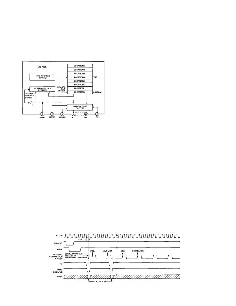
INTERNAL FIFO MEMORY
The internal FIFO memory of the AD7878 consists of eight
memory locations. Each word in memory contains 13 bits of
information—12 bits of data from the conversion result and one
additional bit which contains information as to whether the 12-
bit result is out of range or not. A block diagram of the AD7878
FIFO architecture is shown in Figure 3.
Figure 3. Internal FIFO Architecture
The conversion result is gathered in the successive approxima-
tion register (SAR) during conversion. At the end of conversion
this result is transferred to the FIFO memory. The FIFO ad-
dress pointer always points to the top of memory, which is the
uppermost location containing valid data. The pointer is incre-
mented after each conversion. A read operation from the FIFO
memory accesses data from the bottom of the FIFO, Location 0.
On completion of the read operation, each data word moves
down one location and the address pointer is decremented by
one. Therefore, each conversion result from the SAR enters at
the top of memory, propagates down with successive reads until
it reaches Location 0 from where it can be accessed by a micro-
processor read operation.
The transfer of information from the SAR to the FIFO occurs in
synchronization with the AD7878 input clock (CLK IN). The
propagation of data words down the FIFO is also synchronous
with this clock. As a result, a read operation to obtain data from
the FIFO must also be synchronous with CLK IN to avoid
Read/Write conflicts in the FIFO (i.e., reading from FIFO Loca-
tion 0 while it is being updated). This requires that the micro-
processor clock and the AD7878 CLK IN are derived from the
same source.
INTERNAL COMPARATOR TIMING
The ADC clock, which is applied to CLK IN, controls the suc-
cessive approximation A/D conversion process. This clock is
internally divided by four to yield a bit trial cycle time of 500 ns
min (CLK IN = 8 MHz clock). Each bit decision occurs 25 ns
after the rising edge of this divided clock. The bit decision is
latched by the rising edge of an internal comparator strobe sig-
nal. There are 12-bit decisions, as in a normal successive ap-
proximation routine, and one extra decision that checks if the
input sample is out of range. In a normal successive approxima-
tion A/D converter, reading data from the device during conver-
sion can upset the conversion in progress. This is due to on-chip
transients, generated by charging or discharging the databus,
concurrent with a bit decision. The scheme outlined below and
shown in Figure 4 describes how the AD7878 overcomes this
problem.
The internal comparator strobe on the AD7878 is gated with
both
DMRD
and
DMWR
so that if a read or write operation
occurs when a bit decision is about to be made, the bit decision
point is deferred by one CLK IN cycle. In other words, if
DMRD
or
DMWR
goes low (with
CS
low) at any time during
the CLK IN low time immediately prior to the comparator
strobing edge (t
LOW
of Figure 4), the bit trial is suspended for a
clock cycle. This makes sure that the bit decision is latched at a
time when the AD7878 is not attempting to charge or discharge
the data bus, thereby ensuring that no spurious transients occur
internally near a bit decision point.
The decision point slippage mechanism is shown in Figure 4 for
the MSB decision. Normally, the MSB decision occurs 25 ns
after the fourth rising CLK IN edge after
CONVST
goes high.
However, in the timing diagram of Figure 4,
CS
and
DMRD
or
DMWR
are low in the time period t
LOW
prior to the MSB deci-
sion point on the fourth rising edge. This causes the internal
comparator strobe to be slipped to the fifth rising clock edge.
The AD7878 will again check during a period t
LOW
prior to this
fifth rising clock edge; and if the
CS
and
DMRD
or
DMWR
are
still low, the bit decision point will be slipped a further clock
cycle.
The conversion time for the ADC normally consists of the 13-
bit trials described above and one extra internal clock cycle during
which data is written from the SAR to the FIFO. For an 8 MHz
input clock this results in a conversion time of 7
μ
s. However,
the software routine servicing the AD7878 has the potential to
read 16 times from the device during conversion—8 reads from
the FIFO and 8 reads from the status/control register. It also has
the potential to write once to the status/control register. If these
Figure 4. Operational Timing Diagram
相關PDF資料 |
PDF描述 |
|---|---|
| AD7878SE | LC2MOS Complete 12-Bit 100 kHz Sampling ADC with DSP Interface |
| AD7878LN | SOTiny Low-Voltage, 8-Ohm Single Analog / Bus Switch |
| AD7878LP | IC LOGIC 125 LOW-VOLTAGE SINGLE FET 8-OHM BUS SWITCH -40+85C SC-70-5 3000/REEL |
| AD7878JN | LC2MOS Complete 12-Bit 100 kHz Sampling ADC with DSP Interface |
| AD7878JP | LC2MOS Complete 12-Bit 100 kHz Sampling ADC with DSP Interface |
相關代理商/技術參數 |
參數描述 |
|---|---|
| AD7878KPZ | 功能描述:IC ADC 12BIT W/DSP INT 28-PLCC RoHS:是 類別:集成電路 (IC) >> 數據采集 - 模數轉換器 系列:- 產品培訓模塊:Lead (SnPb) Finish for COTS Obsolescence Mitigation Program 標準包裝:2,500 系列:- 位數:12 采樣率(每秒):3M 數據接口:- 轉換器數目:- 功率耗散(最大):- 電壓電源:- 工作溫度:- 安裝類型:表面貼裝 封裝/外殼:SOT-23-6 供應商設備封裝:SOT-23-6 包裝:帶卷 (TR) 輸入數目和類型:- |
| AD7878KPZ-REEL | 功能描述:IC ADC 12BIT W/DSP 28PLCC RoHS:是 類別:集成電路 (IC) >> 數據采集 - 模數轉換器 系列:- 標準包裝:1 系列:- 位數:14 采樣率(每秒):83k 數據接口:串行,并聯 轉換器數目:1 功率耗散(最大):95mW 電壓電源:雙 ± 工作溫度:0°C ~ 70°C 安裝類型:通孔 封裝/外殼:28-DIP(0.600",15.24mm) 供應商設備封裝:28-PDIP 包裝:管件 輸入數目和類型:1 個單端,雙極 |
| AD7878LN | 功能描述:IC ADC 12BIT W/DSP INT 28-DIP RoHS:否 類別:集成電路 (IC) >> 數據采集 - 模數轉換器 系列:- 標準包裝:1 系列:- 位數:14 采樣率(每秒):83k 數據接口:串行,并聯 轉換器數目:1 功率耗散(最大):95mW 電壓電源:雙 ± 工作溫度:0°C ~ 70°C 安裝類型:通孔 封裝/外殼:28-DIP(0.600",15.24mm) 供應商設備封裝:28-PDIP 包裝:管件 輸入數目和類型:1 個單端,雙極 |
| AD7878LP | 制造商:Analog Devices 功能描述:ADC Single SAR 100ksps 12-bit Parallel 28-Pin PLCC 制造商:Rochester Electronics LLC 功能描述:12-BIT ADC IC - Bulk |
| AD7878LPZ | 功能描述:IC ADC 12BIT W/DSP INT 28-PLCC RoHS:是 類別:集成電路 (IC) >> 數據采集 - 模數轉換器 系列:- 產品培訓模塊:Lead (SnPb) Finish for COTS Obsolescence Mitigation Program 標準包裝:250 系列:- 位數:12 采樣率(每秒):1.8M 數據接口:并聯 轉換器數目:1 功率耗散(最大):1.82W 電壓電源:模擬和數字 工作溫度:-40°C ~ 85°C 安裝類型:表面貼裝 封裝/外殼:48-LQFP 供應商設備封裝:48-LQFP(7x7) 包裝:管件 輸入數目和類型:2 個單端,單極 |
發布緊急采購,3分鐘左右您將得到回復。