- 您現在的位置:買賣IC網 > PDF目錄373923 > AD7880BQ (ANALOG DEVICES INC) LC2MOS Single +5 V Supply, Low Power, 12-Bit Sampling ADC PDF資料下載
參數資料
| 型號: | AD7880BQ |
| 廠商: | ANALOG DEVICES INC |
| 元件分類: | ADC |
| 英文描述: | LC2MOS Single +5 V Supply, Low Power, 12-Bit Sampling ADC |
| 中文描述: | 1-CH 12-BIT SUCCESSIVE APPROXIMATION ADC, PARALLEL ACCESS, CDIP24 |
| 封裝: | 0.300 INCH, HERMETIC SEALED, CERDIP-24 |
| 文件頁數: | 9/16頁 |
| 文件大小: | 337K |
| 代理商: | AD7880BQ |
AD7880
REV. 0
–9–
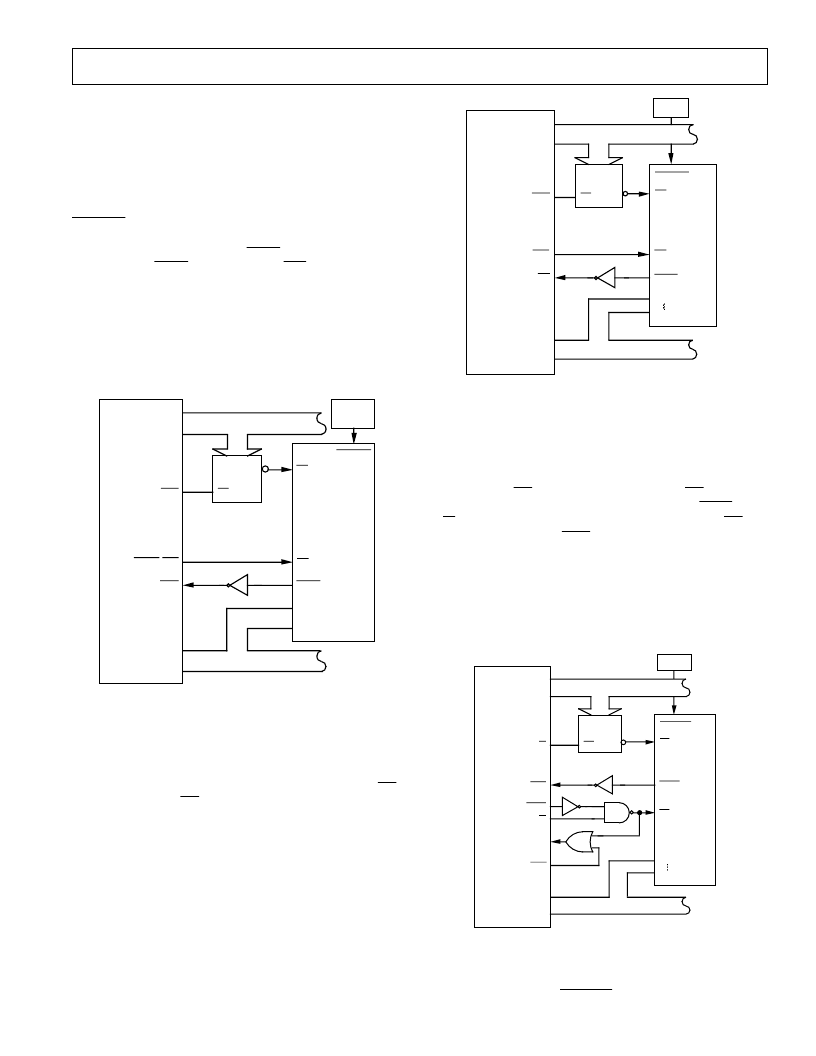
MICROPROCE SSOR INT E RFACING
T he AD7880 high speed bus timing allows direct interfacing to
real time digital signal processors, DSPs, as well as modern high
speed, 16-bit microprocessors. Suitable microprocessor inter-
faces are shown in Figures 15 through 20.
AD7880–ADSP-2100 Interface
Figure 15 shows an interface between the AD7880 and the
ADSP-2100. Conversion is initiated using a timer to drive the
CONVST
input asynchronously to the microprocessor. T his al-
lows very accurate control of the sampling instant. When con-
version is complete, the AD7880
BUSY
line goes high. An
inverter on this
BUSY
output drives the
IRQ
line low thus pro-
viding an interrupt to the ADSP-2100 when conversion is com-
pleted. T he conversion result is then read from the AD7880 into
the ADSP-2100 with the following instruction:
MR0 = DM(ADC)
where
MR0
is
the ADSP-2100 MR0 Register and
where
ADC
is the AD7880 address.
TIMER
DMA0
DMA13
DMD15
DMD0
DMS
EN
ADDR
DECODE
ADDRESS BUS
ADSP-2100
(ADSP-2101/
ADSP-2102)
* ADDITIONAL PINS OMITTED FOR CLARITY
DATA BUS
CONVST
CS
A
RD
BUSY
AD7880*
IRQn
DMRD (RD)
A
Figure 15. AD7880–ADSP-2100 (ADSP-2101/ADSP-2102)
Interface
AD7880-ADSP-2101/ADSP-2102 Interface
T he interface outlined in Figure 15 also forms the basis for an
interface between the AD7880 and the ADSP-2101/ADSP-2102.
T he READ line of the ADSP-2101/ADSP-2102 is labeled
RD
.
In this interface, the
RD
pulse width of the processor can be
programmed using the Data Memory Wait State Control Regis-
ter. T he instruction used to read a conversion result is as out-
lined for the ADSP-2100.
AD7880-T MS32010 Interface
An interface between the AD7880 and the T MS32010 is shown
in Figure 16. Once again the conversion is initiated using an ex-
ternal timer and the T MS32010 is interrupted when conversion
is completed. T he following instruction is used to read the con-
version result from the AD7880:
IN D,ADC
where
D
is
Data Memory Address and
where
ADC
is the AD7880 address.
PA0
PA2
D15
D0
MEN
ADDR
DECODE
ADDRESS BUS
TIMER
DATA BUS
CONVST
CS
A
RD
AD7880*
TMS32010
*ADDITIONAL PINS OMITTED FOR CLARITY
INT
DEN
EN
BUSY
A
Figure 16. AD7880–TMS32010 Interface
AD7880–T MS320C25 Interface
Figure 17 shows an interface between the AD7880 and the
T MS320C25. As with the two previous interfaces, conversion is
initiated with a timer, and the processor is interrupted when the
conversion sequence is completed. T he T MS320C25 does not
have a separate
RD
output to drive the AD7880
RD
input di-
rectly. T his has to be generated from the processor
STRB
and
R/
W
outputs with the addition of some logic gates. T he
RD
sig-
nal is OR-gated with the
MSC
signal to provide the one WAIT
state required in the read cycle for correct interface timing.
Conversion results are read from the AD7880 using the follow-
ing instruction:
IN D,ADC
where
D
is
Data Memory Address and
where
ADC
is the AD7880 address.
A0
A15
D15
D0
IS
EN
ADDR
DECODE
ADDRESS BUS
TIMER
DATA BUS
CONVST
CS
DB11
DB0
RD
AD7880*
TMS320C25
*ADDITIONAL PINS OMITTED FOR CLARITY
INTn
R/W
STRB
MSC
READY
BUSY
Figure 17. AD7880–TMS320C25 Interface
Some applications may require that the conversion be initiated
by the microprocessor rather than an external timer. One option
is to decode the AD7880
CONVST
from the address bus so that
相關PDF資料 |
PDF描述 |
|---|---|
| AD7880BR | LC2MOS Single +5 V Supply, Low Power, 12-Bit Sampling ADC |
| AD7880CN | LC2MOS Single +5 V Supply, Low Power, 12-Bit Sampling ADC |
| AD7880CQ | Enclosed Switches Series LS: Wobble - Steel Wire; 1NC 1NO DPDT Snap Action, Double Break; 0.5 in - 14NPT conduit; Plug-in |
| AD7883 | LC2MOS 12-Bit, 3.3 V Sampling ADC |
| AD7883BN | LC2MOS 12-Bit, 3.3 V Sampling ADC |
相關代理商/技術參數 |
參數描述 |
|---|---|
| AD7880BR | 功能描述:IC ADC 12BIT LC2MOS 5V LP 24SOIC RoHS:否 類別:集成電路 (IC) >> 數據采集 - 模數轉換器 系列:- 標準包裝:1 系列:- 位數:14 采樣率(每秒):83k 數據接口:串行,并聯 轉換器數目:1 功率耗散(最大):95mW 電壓電源:雙 ± 工作溫度:0°C ~ 70°C 安裝類型:通孔 封裝/外殼:28-DIP(0.600",15.24mm) 供應商設備封裝:28-PDIP 包裝:管件 輸入數目和類型:1 個單端,雙極 |
| AD7880BR-REEL | 功能描述:IC ADC 12BIT MONO LP 24-SOIC RoHS:否 類別:集成電路 (IC) >> 數據采集 - 模數轉換器 系列:- 標準包裝:1 系列:- 位數:14 采樣率(每秒):83k 數據接口:串行,并聯 轉換器數目:1 功率耗散(最大):95mW 電壓電源:雙 ± 工作溫度:0°C ~ 70°C 安裝類型:通孔 封裝/外殼:28-DIP(0.600",15.24mm) 供應商設備封裝:28-PDIP 包裝:管件 輸入數目和類型:1 個單端,雙極 |
| AD7880BRZ | 功能描述:IC ADC 12BIT MONO LP 24-SOIC RoHS:是 類別:集成電路 (IC) >> 數據采集 - 模數轉換器 系列:- 其它有關文件:TSA1204 View All Specifications 標準包裝:1 系列:- 位數:12 采樣率(每秒):20M 數據接口:并聯 轉換器數目:2 功率耗散(最大):155mW 電壓電源:模擬和數字 工作溫度:-40°C ~ 85°C 安裝類型:表面貼裝 封裝/外殼:48-TQFP 供應商設備封裝:48-TQFP(7x7) 包裝:Digi-Reel® 輸入數目和類型:4 個單端,單極;2 個差分,單極 產品目錄頁面:1156 (CN2011-ZH PDF) 其它名稱:497-5435-6 |
| AD7880BRZ-REEL | 功能描述:IC ADC 12BIT MONO LP 24-SOIC RoHS:是 類別:集成電路 (IC) >> 數據采集 - 模數轉換器 系列:- 標準包裝:1,000 系列:- 位數:12 采樣率(每秒):300k 數據接口:并聯 轉換器數目:1 功率耗散(最大):75mW 電壓電源:單電源 工作溫度:0°C ~ 70°C 安裝類型:表面貼裝 封裝/外殼:24-SOIC(0.295",7.50mm 寬) 供應商設備封裝:24-SOIC 包裝:帶卷 (TR) 輸入數目和類型:1 個單端,單極;1 個單端,雙極 |
| AD7880CN | 制造商:Analog Devices 功能描述:ADC Single SAR 66ksps 12-bit Parallel 24-Pin PDIP |
發布緊急采購,3分鐘左右您將得到回復。