- 您現在的位置:買賣IC網 > PDF目錄373923 > AD7880CR (ANALOG DEVICES INC) LC2MOS Single +5 V Supply, Low Power, 12-Bit Sampling ADC PDF資料下載
參數資料
| 型號: | AD7880CR |
| 廠商: | ANALOG DEVICES INC |
| 元件分類: | ADC |
| 英文描述: | LC2MOS Single +5 V Supply, Low Power, 12-Bit Sampling ADC |
| 中文描述: | 1-CH 12-BIT SUCCESSIVE APPROXIMATION ADC, PARALLEL ACCESS, PDSO24 |
| 封裝: | SOIC-24 |
| 文件頁數: | 11/16頁 |
| 文件大小: | 337K |
| 代理商: | AD7880CR |
AD7880
REV. 0
–11–
V+
+
–
C1
10μF
C2
0.1μF
IC1
ANALOG
INPUT
V+
V–
A B
A
V–
A B
LK3
LK2
TO ADC
LK1
SKT1
A
C3
10μF
C4
0.1μF
A
V+
V
DD
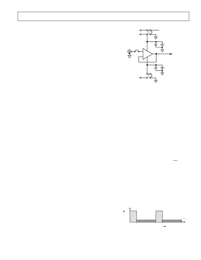
Figure 21. Analog Input Buffering
When it is required to drive the AD7880 with the 0 V to 10 V
input range, an external supply must be connected to V+ (see
Figure 21).
In bipolar operation, positive and negative supplies must be
connected to V+ and V–.
T he AD711 is a general purpose op amp which could be used
to drive the analog input of the AD7880.
POWE R-DOWN CONT ROL (MODE INPUT )
T he AD7880 is designed for systems which need to have mini-
mum power consumption. T his includes such applications as
hand held, portable battery powered systems and remote moni-
toring systems. As well as consuming minimum power under
normal operating conditions, typically 20 mW, the AD7880
can be put into a power-down or sleep mode when not required
to convert signals. When in this power-down mode, the
AD7880 consumes approximately 2 mW of power.
T he AD7880 is powered down by bringing the MODE input
pin to a Logic Low in conjunction with keeping the
RD
input
control High. T he AD7880 will remain in the power-down
mode until MODE is brought to a Logic High again. T he
MODE input should be driven with CD4000 or HCMOS logic
levels.
It is recommended that one “dummy” conversion be imple-
mented before reading conversion data from the AD7880 after
it has been in the power-down mode. T his is required to reset
all internal logic and control circuitry. In a remote monitoring
system where, say, 10 conversions are required to be taken with
a sampling interval of 1 second, an additional 11th conversion
must be carried out. Figure 22 gives a plot of power consumption
2
AA
TIME – secs
POWER
CONSUMPTION – mW
20
2
AAA
1.65 x 10
AAA
POWER-DOWN
4
–
AAA
AAA
AAA
AAA
AAA
AAA
Figure 22. Power Consumption for Normal Operation
and Power-Down Operation vs. Time
APPLICAT ION HINT S
Good printed circuit board (PCB) layout is as important as the
circuit design itself in achieving high speed A/D performance.
T he AD7880’s comparator is required to make bit decisions on
an LSB size of 1.22 mV. T o achieve this, the designer must be
conscious of noise both in the ADC itself and in the preceding
analog circuitry. Switching mode power supplies are not recom-
mended, as the switching spikes will feed through to the com-
parator causing noisy code transitions. Other causes of concern
are ground loops and digital feedthrough from microprocessors.
T hese are factors which influence any ADC, and a proper PCB
layout which minimizes these effects is essential for best
performance.
LAY OUT HINT S
Ensure that the layout for the printed circuit board has the digi-
tal and analog signal lines separated as much as possible. T ake
care not to run digital tracks alongside analog signal tracks.
Guard (screen) the analog input with AGND.
Establish a single point analog ground (star ground) separate
from the logic system ground at the AD7880 AGND pin or as
close as possible to the AD7880. Connect all other grounds and
the AD7880 DGND to this single analog ground point. Do not
connect any other digital grounds to this analog ground point.
Low impedance analog and digital power supply common re-
turns are essential to low noise operation of the ADC, so make
the foil width for these tracks as wide as possible. T he use of
ground planes minimizes impedance paths and also guards the
analog circuitry from digital noise. T he circuit layout of Fig-
ures 26 and 27 have both analog and digital ground planes
which are kept separated and only joined together at the
AD7880 AGND pin.
NOISE
K eep the input signal leads to V
IN
and signal return leads from
AGND as short as possible to minimize input noise coupling. In
applications where this is not possible, use a shielded cable be-
tween the source and the ADC. Reduce the ground circuit im-
pedance as much as possible since any potential difference in
grounds between the signal source and the ADC appears as an
error voltage in series with the input signal.
ANALOG INPUT BUFFE RING
T o achieve specified performance, it is recommended that the
analog input (V
INA
, V
INB
) be driven from a low impedance
source. T his necessitates the use of an input buffer amplifier.
T he choice of op amp will be a function of the particular appli-
cation and the desired analog input range. T he data acquisition
circuit, described in this data sheet allows for various op amp
configurations. Figure 21 shows the analog input buffer circuit.
T he options available to drive the supply of the op amp are:
Single +5 V (derived from PCB 5 V supply)
Dual Supply (externally supplied to V+ and V–)
±
5 V,
±
12 V or
±
15 V
T he simplest configuration is the 0 V to 5 V range of Figure 5.
A single supply 5 V op amp is recommended for such an imple-
mentation. T his will allow for operation of the AD7880 in the 0
V to 5 V unipolar range without supplying an external supply to
V+ and V–. T he 5 V supply is derived from the systems
+5 V V
DD
supply.
相關PDF資料 |
PDF描述 |
|---|---|
| AD7880BN | LC2MOS Single +5 V Supply, Low Power, 12-Bit Sampling ADC |
| AD7880BQ | LC2MOS Single +5 V Supply, Low Power, 12-Bit Sampling ADC |
| AD7880BR | LC2MOS Single +5 V Supply, Low Power, 12-Bit Sampling ADC |
| AD7880CN | LC2MOS Single +5 V Supply, Low Power, 12-Bit Sampling ADC |
| AD7880CQ | Enclosed Switches Series LS: Wobble - Steel Wire; 1NC 1NO DPDT Snap Action, Double Break; 0.5 in - 14NPT conduit; Plug-in |
相關代理商/技術參數 |
參數描述 |
|---|---|
| AD7880CR-REEL | 制造商:Analog Devices 功能描述:ADC Single SAR 66ksps 12-bit Parallel 24-Pin SOIC W T/R 制造商:Analog Devices 功能描述:ADC SGL SAR 66KSPS 12-BIT PARALLEL 24SOIC W - Tape and Reel |
| AD7880CRZ | 功能描述:IC ADC 12BIT MONO LP 24-SOIC RoHS:是 類別:集成電路 (IC) >> 數據采集 - 模數轉換器 系列:- 其它有關文件:TSA1204 View All Specifications 標準包裝:1 系列:- 位數:12 采樣率(每秒):20M 數據接口:并聯 轉換器數目:2 功率耗散(最大):155mW 電壓電源:模擬和數字 工作溫度:-40°C ~ 85°C 安裝類型:表面貼裝 封裝/外殼:48-TQFP 供應商設備封裝:48-TQFP(7x7) 包裝:Digi-Reel® 輸入數目和類型:4 個單端,單極;2 個差分,單極 產品目錄頁面:1156 (CN2011-ZH PDF) 其它名稱:497-5435-6 |
| AD7880CRZ-REEL | 功能描述:IC ADC 12BIT MONO LP 24-SOIC RoHS:是 類別:集成電路 (IC) >> 數據采集 - 模數轉換器 系列:- 標準包裝:1 系列:- 位數:14 采樣率(每秒):83k 數據接口:串行,并聯 轉換器數目:1 功率耗散(最大):95mW 電壓電源:雙 ± 工作溫度:0°C ~ 70°C 安裝類型:通孔 封裝/外殼:28-DIP(0.600",15.24mm) 供應商設備封裝:28-PDIP 包裝:管件 輸入數目和類型:1 個單端,雙極 |
| AD7883BN | 制造商:Analog Devices 功能描述:ADC Single SAR 50ksps 12-bit Parallel 24-Pin SOIC W 制造商:Rochester Electronics LLC 功能描述:12 BIT A/D CONVERTER IC - Bulk |
| AD7883BR | 制造商:Analog Devices 功能描述:ADC Single SAR 50ksps 12-bit Parallel 24-Pin SOIC W 制造商:Analog Devices 功能描述:ADC SGL SAR 50KSPS 12-BIT PARALLEL 24SOIC W - Rail/Tube 制造商:Rochester Electronics LLC 功能描述:12 BIT A/D CONVERTER IC - Bulk |
發布緊急采購,3分鐘左右您將得到回復。