- 您現在的位置:買賣IC網 > PDF目錄373923 > AD7883 (Analog Devices, Inc.) LC2MOS 12-Bit, 3.3 V Sampling ADC PDF資料下載
參數資料
| 型號: | AD7883 |
| 廠商: | Analog Devices, Inc. |
| 英文描述: | LC2MOS 12-Bit, 3.3 V Sampling ADC |
| 中文描述: | LC2MOS 12位,3.3伏采樣ADC |
| 文件頁數: | 4/12頁 |
| 文件大小: | 349K |
| 代理商: | AD7883 |
AD7883
REV. 0
–4–
ABSOLUTE MAXIMUM RATINGS*
V
DD
to AGND . . . . . . . . . . . . . . . . . . . . . . . . . –0.3 V to +7 V
V
DD
to DGND . . . . . . . . . . . . . . . . . . . . . . . . . –0.3 V to +7 V
AGND to DGND . . . . . . . . . . . . . . . . –0.3 V to V
DD
+ 0.3 V
V
INA
, V
INB
to AGND (Figure 4) . . . . . –0.3 V to V
DD
+ 0.3 V
V
INA
to AGND (Figure 5) . . . . . . –V
DD
–0.3 V to V
DD
+ 0.3 V
V
REF
to AGND . . . . . . . . . . . . . . . . . . . . . . . . . . 0.3 V to V
DD
Digital Inputs to DGND . . . . . . . . . . . –0.3 V to V
DD
+ 0.3 V
Digital Outputs to DGND . . . . . . . . . . –0.3 V to V
DD
+ 0.3 V
Operating Temperature Range
Industrial (B Version) . . . . . . . . . . . . . . . . –40
°
C to +85
°
C
Storage Temperature Range . . . . . . . . . . . –65
°
C to +150
°
C
Lead Temperature (Soldering, 10 secs) . . . . . . . . . . . .+300
°
C
Power Dissipation (Any Package) to +75
°
C . . . . . . . 450 mW
Derates above +75
°
C by . . . . . . . . . . . . . . . . . . . . 10 mW/
°
C
*Stresses above those listed under “Absolute Maximum Ratings” may cause
permanent damage to the device. This is a stress rating only and functional
operation of the device at these or any other conditions above those listed in the
operational sections of this specification is not implied. Exposure to absolute
maximum rating conditions for extended periods may affect device reliability.
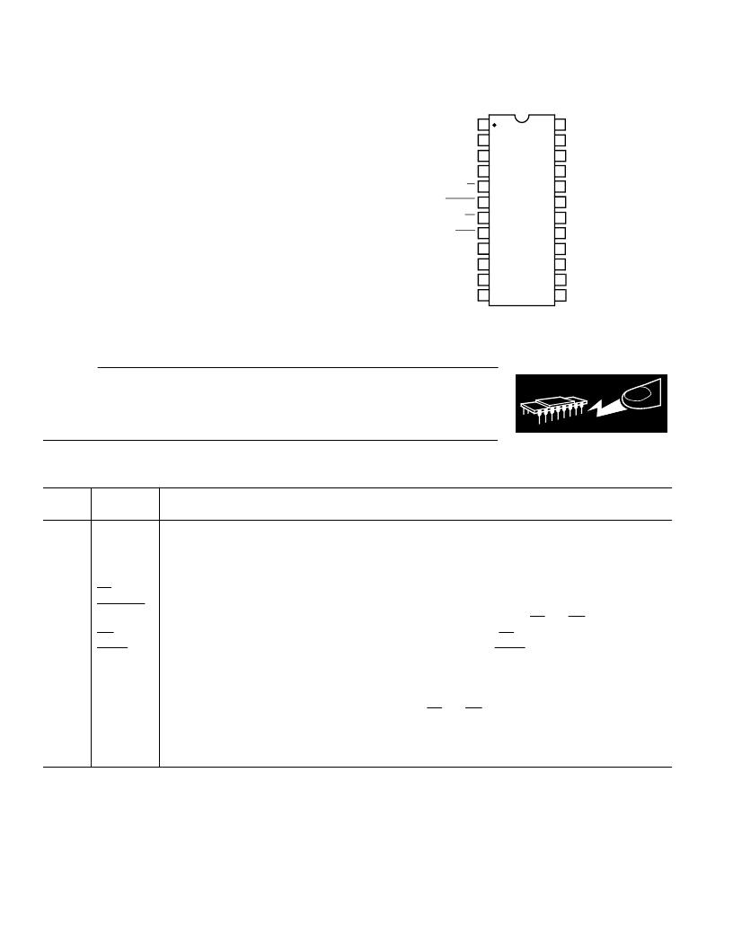
PIN CONFIGURATION
TOP VIEW
(Not to Scale)
1
2
3
4
5
6
7
8
9
10
11
12
13
14
24
23
22
21
20
19
18
17
16
15
AD7883
AGND
CLKIN
DGND
DB0
DB1
DB2
DB3
DB4
DB5
DB6
V
DD
DB8
V
INA
V
INB
DB7
DB9
DB10
DB11
MODE
CS
CONVST
RD
BUSY
V
REF
WARNING!
ESD SENSITIVE DEVICE
CAUTION
ESD (electrostatic discharge) sensitive device. Electrostatic charges as high as 4000 V readily
accumulate on the human body and test equipment and can discharge without detection.
Although the AD7883 features proprietary ESD protection circuitry, permanent damage may
occur on devices subjected to high energy electrostatic discharges. Therefore, proper ESD
precautions are recommended to avoid performance degradation or loss of functionality.
PIN FUNCTION DESCRIPTION
Pin
No.
Pin
Mnemonic
Function
1
1
1
2
1
3
1
4
1
5
1
6
V
INA
V
INB
AGND
V
REF
CS
CONVST
Analog Input.
Analog Input.
Analog Ground.
Voltage Reference Input. This is normally tied to V
DD.
Chip Select. Active Low Logic input. The device is selected when this input is active.
Convert Start. A low to high transition on this input puts the track/hold into hold mode and starts
conversion. This input is asynchronous to the CLKIN and is independent of
CS
and
RD
.
Read. Active Low Logic Input. This input is used in conjunction with
CS
low to enable data outputs.
Active Low Logic Output. This status line indicates converter status.
BUSY
is low during conversion.
Clock Input. TTL-compatible logic input. Used as the clock source for the A/D converter. The mark/
space ratio of the clock can vary from 40/60 to 60/40.
Digital Ground.
Three-State Data Outputs. These become active when
CS
and
RD
are brought low.
MODE Input. This input is used to put the device into the power save mode (MODE = 0 V). During
normal operation, the MODE input will be a logic high (MODE = V
DD
).
Power Supply. This is nominally +3.3 V.
1
7
1
8
1
9
RD
BUSY
CLKIN
10
11 . . . 22 DB0–DB11
23
MODE
DGND
24
V
DD
相關PDF資料 |
PDF描述 |
|---|---|
| AD7883BN | LC2MOS 12-Bit, 3.3 V Sampling ADC |
| AD7883BR | LC2MOS 12-Bit, 3.3 V Sampling ADC |
| AD7884 | LC2MOS 16-Bit, High Speed Sampling ADCs |
| AD7884AN | LC2MOS 16-Bit, High Speed Sampling ADCs |
| AD7884AP | LC2MOS 16-Bit, High Speed Sampling ADCs |
相關代理商/技術參數 |
參數描述 |
|---|---|
| AD7883BN | 制造商:Analog Devices 功能描述:ADC Single SAR 50ksps 12-bit Parallel 24-Pin SOIC W 制造商:Rochester Electronics LLC 功能描述:12 BIT A/D CONVERTER IC - Bulk |
| AD7883BR | 制造商:Analog Devices 功能描述:ADC Single SAR 50ksps 12-bit Parallel 24-Pin SOIC W 制造商:Analog Devices 功能描述:ADC SGL SAR 50KSPS 12-BIT PARALLEL 24SOIC W - Rail/Tube 制造商:Rochester Electronics LLC 功能描述:12 BIT A/D CONVERTER IC - Bulk |
| AD7883BR-REEL | 制造商:Analog Devices 功能描述:ADC Single SAR 50ksps 12-bit Parallel 24-Pin SOIC W T/R 制造商:Analog Devices 功能描述:ADC SGL SAR 50KSPS 12-BIT PARALLEL 24SOIC W - Tape and Reel 制造商:Rochester Electronics LLC 功能描述:12 BIT A/D CONVERTER IC - Tape and Reel |
| AD7884AP | 制造商:Analog Devices 功能描述:ADC Single 2-Step Flash 166ksps 16-bit Parallel 44-Pin PLCC 制造商:Rochester Electronics LLC 功能描述:16-BIT PARAL.SAMPL.ADC IC - Bulk |
| AD7884AP-REEL | 制造商:Analog Devices 功能描述:ADC Single 2-Step Flash 166ksps 16-bit Parallel 44-Pin PLCC T/R 制造商:Rochester Electronics LLC 功能描述:16-BIT PARAL.SAMPL ADC IC - Tape and Reel |
發布緊急采購,3分鐘左右您將得到回復。