- 您現在的位置:買賣IC網 > PDF目錄373923 > AD7883BR (ANALOG DEVICES INC) LC2MOS 12-Bit, 3.3 V Sampling ADC PDF資料下載
參數資料
| 型號: | AD7883BR |
| 廠商: | ANALOG DEVICES INC |
| 元件分類: | ADC |
| 英文描述: | LC2MOS 12-Bit, 3.3 V Sampling ADC |
| 中文描述: | 1-CH 12-BIT SUCCESSIVE APPROXIMATION ADC, PARALLEL ACCESS, PDSO24 |
| 封裝: | SOIC-24 |
| 文件頁數: | 7/12頁 |
| 文件大小: | 349K |
| 代理商: | AD7883BR |
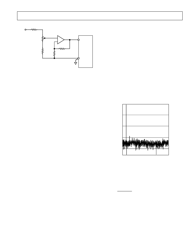
AD7883
REV. 0
–7–
+
–
V
1
R1
10k
V
INA
AGND
AD7883*
R2
500
R3
10k
R5
10k
R4
10k
*ADDITIONAL PINS OMITTED FOR CLARITY
Figure 9. Offset and Full-Scale Adjust Circuit
Unipolar Adjustments
In the case of the 0 V to 3.3 V unipolar input configuration, uni-
polar offset error must be adjusted before full-scale error. Ad-
justment is achieved by trimming the offset of the op amp
driving the analog input of the AD7883. This is done by apply-
ing an input voltage of 0.4 mV (1/2 LSB) to V
1
in Figure 9 and
adjusting the op amp offset voltage until the ADC output code
flickers between 0000 0000 0000 and 0000 0000 0001. For full-
scale adjustment, an input voltage of 3.2988 V (FS–3/2 LSBs) is
applied to V
1
and R2 is adjusted until the output code flickers
between 1111 1111 1110 and 1111 1111 1111.
Bipolar Adjustments
Bipolar zero and full-scale errors for the bipolar input configura-
tion of Figure 5 are adjusted in a similar fashion to the unipolar
case. Again, bipolar zero error must be adjusted before full-scale
error. Bipolar zero error adjustment is achieved by trimming the
offset of the op amp driving the analog input of the AD7883
while the input voltage is 1/2 LSB below ground. This is done
by applying an input voltage of –0.8 mV (1/2 LSB) to V
1
in Fig-
ure 9 and adjusting the op amp offset voltage until the ADC
output code flickers between 0111 1111 1111 and 1000 0000
0000. For full-scale adjustment, an input voltage of 3.2988 V
(FS/2–3/2 LSBs) is applied to V
1
and R2 is adjusted until the
output code flickers between 1111 1111 1110 and 1111 1111
1111.
DYNAMIC SPECIFICATIONS
The AD7883 is specified and tested for dynamic performance
specifications as well as traditional dc specifications such as inte-
gral and differential nonlinearity. The ac specifications are re-
quired for signal processing applications such as speech
recognition, spectrum analysis and high speed modems. These
applications require information on the ADC’s effect on the
spectral content of the input signal. Hence, the parameters for
which the AD7883 is specified include SNR, harmonic distor-
tion, intermodulation distortion and peak harmonics. These
terms are discussed in more detail in the following sections.
Signal-to-Noise Ratio (SNR)
SNR is the measured signal-to-noise ratio at the output of the
ADC. The signal is the rms magnitude of the fundamental.
Noise is the rms sum of all the nonfundamental signals up to
half the sampling frequency (FS/2) excluding dc. SNR is depen-
dent upon the number of quantization levels used in the digiti-
zation process; the more levels, the smaller the quantization
noise. The theoretical signal to noise ratio for a sine wave input
is given by:
SNR
= (6.02
N
+ 1.76)
dB
where
N
is the number of bits.
Thus for an ideal 12-bit converter, SNR = 74 dB.
The output spectrum from the ADC is evaluated by applying a
sine wave signal of very low distortion to the V
IN
input which is
sampled at a 50 kHz sampling rate. A Fast Fourier Transform
(FFT) plot is generated from which the SNR data can be ob-
tained. Figure 10 shows a typical 2048 point FFT plot of the
AD7883 with an input signal of 2.5 kHz and a sampling fre-
quency of 50 kHz. The SNR obtained from this graph is 71 dB.
It should be noted that the harmonics are taken into account
when calculating the SNR.
(1)
0
–30
–60
–90
–120
0
2.5
25
FREQUENCY – kHz
S
INPUT FREQUENCY = 2.5kHz
SAMPLE FREQUENCY = 50kHz
SNR = 71.4dB
T
A
= +25°C
Figure 10. FFT Plot
Effective Number of Bits
The formula given in Equation 1 relates the SNR to the number
of bits. Rewriting the formula, as in Equation 2, it is possible to
get a measure of performance expressed in effective number of
bits (N).
N
=
SNR
–1.76
The effective number of bits for a device can be calculated di-
rectly from its measured SNR.
Figure 11 shows a plot of effective number of bits versus input
frequency for an AD7883 with a sampling frequency of 50 kHz.
The effective number of bits typically remains better than 11.5
for frequencies up to 12 kHz.
6.02
(2)
相關PDF資料 |
PDF描述 |
|---|---|
| AD7884 | LC2MOS 16-Bit, High Speed Sampling ADCs |
| AD7884AN | LC2MOS 16-Bit, High Speed Sampling ADCs |
| AD7884AP | LC2MOS 16-Bit, High Speed Sampling ADCs |
| AD7884BN | LC2MOS 16-Bit, High Speed Sampling ADCs |
| AD7884BP | LC2MOS 16-Bit, High Speed Sampling ADCs |
相關代理商/技術參數 |
參數描述 |
|---|---|
| AD7883BR-REEL | 制造商:Analog Devices 功能描述:ADC Single SAR 50ksps 12-bit Parallel 24-Pin SOIC W T/R 制造商:Analog Devices 功能描述:ADC SGL SAR 50KSPS 12-BIT PARALLEL 24SOIC W - Tape and Reel 制造商:Rochester Electronics LLC 功能描述:12 BIT A/D CONVERTER IC - Tape and Reel |
| AD7884AP | 制造商:Analog Devices 功能描述:ADC Single 2-Step Flash 166ksps 16-bit Parallel 44-Pin PLCC 制造商:Rochester Electronics LLC 功能描述:16-BIT PARAL.SAMPL.ADC IC - Bulk |
| AD7884AP-REEL | 制造商:Analog Devices 功能描述:ADC Single 2-Step Flash 166ksps 16-bit Parallel 44-Pin PLCC T/R 制造商:Rochester Electronics LLC 功能描述:16-BIT PARAL.SAMPL ADC IC - Tape and Reel |
| AD7884APZ | 功能描述:IC ADC 16BIT SAMPLING HS 44PLCC RoHS:是 類別:集成電路 (IC) >> 數據采集 - 模數轉換器 系列:- 產品培訓模塊:Lead (SnPb) Finish for COTS Obsolescence Mitigation Program 標準包裝:250 系列:- 位數:12 采樣率(每秒):1.8M 數據接口:并聯 轉換器數目:1 功率耗散(最大):1.82W 電壓電源:模擬和數字 工作溫度:-40°C ~ 85°C 安裝類型:表面貼裝 封裝/外殼:48-LQFP 供應商設備封裝:48-LQFP(7x7) 包裝:管件 輸入數目和類型:2 個單端,單極 |
| AD7884APZ-REEL | 功能描述:IC ADC 16BIT SAMPLING HS 44PLCC RoHS:是 類別:集成電路 (IC) >> 數據采集 - 模數轉換器 系列:- 標準包裝:1 系列:- 位數:14 采樣率(每秒):83k 數據接口:串行,并聯 轉換器數目:1 功率耗散(最大):95mW 電壓電源:雙 ± 工作溫度:0°C ~ 70°C 安裝類型:通孔 封裝/外殼:28-DIP(0.600",15.24mm) 供應商設備封裝:28-PDIP 包裝:管件 輸入數目和類型:1 個單端,雙極 |
發布緊急采購,3分鐘左右您將得到回復。