- 您現在的位置:買賣IC網 > PDF目錄373923 > AD7885BN (ANALOG DEVICES INC) LC2MOS 16-Bit, High Speed Sampling ADCs PDF資料下載
參數資料
| 型號: | AD7885BN |
| 廠商: | ANALOG DEVICES INC |
| 元件分類: | ADC |
| 英文描述: | LC2MOS 16-Bit, High Speed Sampling ADCs |
| 中文描述: | 1-CH 16-BIT FLASH METHOD ADC, PARALLEL ACCESS, PDIP28 |
| 封裝: | PLASTIC, DIP-28 |
| 文件頁數: | 5/16頁 |
| 文件大小: | 319K |
| 代理商: | AD7885BN |
AD7884/AD7885
REV. C
–5–
ABSOLUT E MAX IMUM RAT INGS
1
V
DD
to AGND . . . . . . . . . . . . . . . . . . . . . . . . . –0.3 V to +7 V
AV
DD
to AGND . . . . . . . . . . . . . . . . . . . . . . . . –0.3 V to +7 V
V
SS
to AGND . . . . . . . . . . . . . . . . . . . . . . . . . +0.3 V to –7 V
AV
SS
to AGND . . . . . . . . . . . . . . . . . . . . . . . . –0.3 V to –7 V
AGND Pins to DGND . . . . . . . . . . . . –0.3 V to V
DD
+ 0.3 V
AV
DD
to V
DD2
. . . . . . . . . . . . . . . . . . . . . . . . . –0.3 V to +7 V
AV
SS
to V
SS2
. . . . . . . . . . . . . . . . . . . . . . . . . . +0.3 V to –7 V
GND to DGND . . . . . . . . . . . . . . . . . –0.3 V to V
DD
+ 0.3 V
V
IN
S, V
IN
F to AGND . . . . . . . . . . V
SS
–0.3 V to V
DD
+ 0.3 V
V
REF+
to AGND . . . . . . . . . . . . . . . V
SS
–0.3 V to V
DD
+ 0.3 V
V
REF–
to AGND . . . . . . . . . . . . . . . V
SS
–0.3 V to V
DD
+ 0.3 V
V
INV
to AGND . . . . . . . . . . . . . . . V
SS
–0.3 V to V
DD
+ 0.3 V
Digital Inputs to DGND . . . . . . . . . . . –0.3 V to V
DD
+ 0.3 V
Digital Outputs to DGND . . . . . . . . . . –0.3 V to V
DD
+ 0.3 V
Operating T emperature Range
Commercial Plastic (A, B Versions) . . . . . –40
°
C to +85
°
C
Industrial Cerdip (A, B Versions) . . . . . . . . –40
°
C to +85
°
C
Extended Cerdip (T Versions) . . . . . . . . –55
°
C to +125
°
C
Storage T emperature Range . . . . . . . . . . . –65
°
C to +150
°
C
Lead T emperature (Soldering, 10 secs) . . . . . . . . . . . +300
°
C
Power Dissipation (Any Package) to +75
°
C . . . . . . . 1000 mW
Derates above +75
°
C by . . . . . . . . . . . . . . . . . . . . 10 mW/
°
C
1
Stresses above those listed under “Absolute Maximum Ratings” may cause
permanent damage to the device. T his is a stress rating only and functional
operation of the device at these or any other conditions above those listed in the
operational sections of this specification is not implied. Exposure to absolute
maximum rating conditions for extended periods may affect device reliability.
2
If the AD7884/AD7885 is being powered from separate analog and digital supplies,
AV
should always come up before V
SS
. See Figure 12 for a recommended
protection circuit using Schottky diodes.
WARNING!
ESD SENSITIVE DEVICE
C AUT ION
ESD (electrostatic discharge) sensitive device. Electrostatic charges as high as 4000 V readily
accumulate on the human body and test equipment and can discharge without detection.
Although these devices feature proprietary ESD protection circuitry, permanent damage may
occur on devices subjected to high energy electrostatic discharges. T herefore, proper ESD
precautions are recommended to avoid performance degradation or loss of functionality.
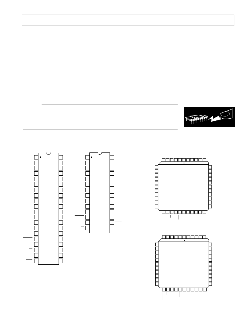
PIN CONFIGURAT IONS
DIP
DB2
DB1
DB0
DB13
DGND
DB11
AV
SS
V
DD
DB7
DB6
DB5
DB4
DB3
CS
RD
BUSY
DB8
DB9
DB10
DB12
V
DD
DB15
DB14
V
INV
V S
V F
V
REF–
AGNDS
AGNDF
AV
DD
V
SS
GND
V
SS
±
3V S
V
SS
CONVST
GND
1
2
3
4
5
6
7
8
9
10
40
39
38
37
36
35
34
33
32
31
TOP VIEW
(Not to Scale)
AD7884
30
29
28
27
26
25
24
23
22
21
11
12
13
14
15
16
17
18
19
20
±
3V F
±
5V S
±
5V F
1
2
3
7
28
27
26
22
8
9
10
21
20
19
11
12
18
17
4
5
25
24
6
23
TOP VIEW
(Not to Scale)
13
14
16
15
AD7885
AV
SS
V
DD
CS
RD
V
INV
V
REF–
AGNDS
AGNDF
AV
DD
GND
±
3V
IN
V
SS
CONVST
±
5V S
±
5V F
DB2
DB1
DB0
DGND
DB7
DB6
DB5
DB4
DB3
V S
V F
BUSY
HBEN
PLCC
±5V
IN
F
±
I
F
AD7884
TOP VIEW
(Not to Scale)
2
1
44
3
4
5
6
42
41
40
43
18
19
20
21
22
23
24
25
26
27
28
39
38
37
36
35
34
33
32
31
30
29
7
8
9
10
11
12
13
14
15
16
17
DGND
DB11
AV
DD
AV
SS
DB7
DB6
DB5
D
D
D
D
D
DB8
DB9
DB10
DB12
D
D
D
V
R
S
V
R
F
AGNDS
AGNDF
V
SS
GND
C
R
B
C
GND
V
I
V
R
±
I
S
±
I
S
NC
NC
N
N
NC = NO CONNECT
V
SS
V
DD
V
S
V
DD
AD7885A
TOP VIEW
(Not to Scale)
2
1
44
3
4
5
6
42
41 40
43
18
19
20
21
22
23
24
25
26
27
28
39
38
37
36
35
34
33
32
31
30
29
7
8
9
10
11
12
13
14
15
16
17
DGND
DB6
DB3
DB2
DB1
D
DB4
DB5
NC
DB7
V
DD
N
N
N
AGNDS
AGNDF
GND
C
R
B
H
C
GND
NC
NC
N
N
NC = NO CONNECT
N
N
N
N
±5V
IN
F
AV
DD
AV
SS
V
SS
V
SS
V
DD
±
I
F
V
R
S
V
R
F
V
I
V
R
±
I
S
±
I
S
相關PDF資料 |
PDF描述 |
|---|---|
| AD7886JP | LC2MOS 12-Bit, 750 kHz/1 MHz, Sampling ADC |
| AD7886 | LC2MOS 12-Bit, 750 kHz/1 MHz, Sampling ADC |
| AD7886BD | LC2MOS 12-Bit, 750 kHz/1 MHz, Sampling ADC |
| AD7886KD | LC2MOS 12-Bit, 750 kHz/1 MHz, Sampling ADC |
| AD7886KP | LC2MOS 12-Bit, 750 kHz/1 MHz, Sampling ADC |
相關代理商/技術參數 |
參數描述 |
|---|---|
| AD7885BQ | 制造商:Analog Devices 功能描述: |
| AD7885JQ | 制造商:Analog Devices 功能描述: 制造商:Rochester Electronics LLC 功能描述: |
| AD7886JD | 功能描述:IC ADC 12BIT SAMPLING HS 28-CDIP RoHS:否 類別:集成電路 (IC) >> 數據采集 - 模數轉換器 系列:- 產品培訓模塊:Lead (SnPb) Finish for COTS Obsolescence Mitigation Program 標準包裝:250 系列:- 位數:12 采樣率(每秒):1.8M 數據接口:并聯 轉換器數目:1 功率耗散(最大):1.82W 電壓電源:模擬和數字 工作溫度:-40°C ~ 85°C 安裝類型:表面貼裝 封裝/外殼:48-LQFP 供應商設備封裝:48-LQFP(7x7) 包裝:管件 輸入數目和類型:2 個單端,單極 |
| AD7886JP | 功能描述:IC ADC 12BIT SAMPLING HS 28-PLCC RoHS:否 類別:集成電路 (IC) >> 數據采集 - 模數轉換器 系列:- 標準包裝:1 系列:- 位數:14 采樣率(每秒):83k 數據接口:串行,并聯 轉換器數目:1 功率耗散(最大):95mW 電壓電源:雙 ± 工作溫度:0°C ~ 70°C 安裝類型:通孔 封裝/外殼:28-DIP(0.600",15.24mm) 供應商設備封裝:28-PDIP 包裝:管件 輸入數目和類型:1 個單端,雙極 |
| AD7886JP-REEL | 功能描述:IC ADC 12BIT SAMPLING HS 28-PLCC RoHS:否 類別:集成電路 (IC) >> 數據采集 - 模數轉換器 系列:- 標準包裝:1 系列:- 位數:14 采樣率(每秒):83k 數據接口:串行,并聯 轉換器數目:1 功率耗散(最大):95mW 電壓電源:雙 ± 工作溫度:0°C ~ 70°C 安裝類型:通孔 封裝/外殼:28-DIP(0.600",15.24mm) 供應商設備封裝:28-PDIP 包裝:管件 輸入數目和類型:1 個單端,雙極 |
發布緊急采購,3分鐘左右您將得到回復。