- 您現在的位置:買賣IC網 > PDF目錄373923 > AD7886BD (ANALOG DEVICES INC) LC2MOS 12-Bit, 750 kHz/1 MHz, Sampling ADC PDF資料下載
參數資料
| 型號: | AD7886BD |
| 廠商: | ANALOG DEVICES INC |
| 元件分類: | ADC |
| 英文描述: | LC2MOS 12-Bit, 750 kHz/1 MHz, Sampling ADC |
| 中文描述: | 1-CH 12-BIT FLASH METHOD ADC, PARALLEL ACCESS, CDIP28 |
| 封裝: | SIDE BRAZED, CERAMIC, DIP-28 |
| 文件頁數: | 10/16頁 |
| 文件大小: | 400K |
| 代理商: | AD7886BD |
AD7886
–10–
REV. B
determined by the largest harmonic in the spectrum, but for
parts where the harmonics are buried in the noise floor, the peak
will be a noise peak.
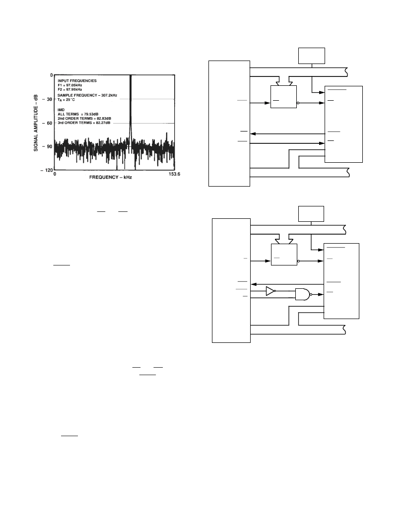
Figure 14. AD7886 IMD Plot
MICROPROCESSOR INTERFACING
The AD7886 is designed to interface to microprocessors as a
memory mapped device. Its
CS
and
RD
control inputs are com-
mon to all memory peripheral interfacing. Figures 15 to 21
demonstrate typical interfaces for the AD7886.
AD7886–TMS320C10/TMS32020
Figures 15 and 16 show typical interfaces for the TMS320C10
and the TMS32020 DSP processors. An external timer controls
conversion start to the processor. At the end of each conversion,
the ADC’s
BUSY
output interrupts the microprocessor. The
conversion result can then be read from the ADC with the fol-
lowing instruction:
IN D,ADC (ADC = ADC address)
AD788S ADSP-2100/TMS320C25/DSP56000
Some of the faster DSP processors have data access times out-
side the capabilities of the AD7886. Interfacing to such proces-
sors requires the use of either a single WAIT state or external
latches. Examples are shown in Figures 17, 18 and 19.
The use of a single WAIT state for the TMS320C25 and the
ADSP-2100 interfaces extends the read instruction to the ADC
by one processor CLK OUT cycle. In the DSP56000 example,
the ADC’s data is first clocked into 74HC374 latches before be-
ing read by the processor. The AD7886’s
CS
and
RD
inputs are
tied permanently low, and the rising edge of
BUSY
updates the
latches at the end of conversion. Both methods of overcoming
the very fast data access time required by these processors are
interchangeable, i.e., a WAIT state can be used for the DSP56000,
eliminating the need for latches or vice or versa, for the other
two interfaces.
For all three interfaces, an external timer controls conversion
start; the processor is interrupted at the end of each conversion
by the ADC’s
BUSY
output. The following instruction then
reads data from the ADC:
ADSP-2100 – MR = DM(ADC)
TMS320C25 – IN D,ADC
DSP56000 – MOVEP Y:ADC,XO
Assuming the ADC is memory mapped into the top
64 locations in Y memory space. (ADC = ADC address)
PA0
PA2
D15
D0
MEN
ADDRESS BUS
TIMER
DATA BUS
CONVST
CS
DB11
DB0
RD
BUSY
AD7886*
TMS320C10
*ADDITIONAL PINS OMITTED FOR CLARITY
INT
DEN
EN
ADDR
ENCODE
Figure 15. AD7886-TMS320C10 Interface
A0
A15
D15
D0
IS
EN
ADDR
ENCODE
ADDRESS BUS
TIMER
DATA BUS
CONVST
CS
DB11
DB0
RD
BUSY
AD7886*
TMS32020
*ADDITIONAL PINS OMITTED FOR CLARITY
INTn
STRB
R/W
Figure 16. AD7886-TMS32020 Interface
相關PDF資料 |
PDF描述 |
|---|---|
| AD7886KD | LC2MOS 12-Bit, 750 kHz/1 MHz, Sampling ADC |
| AD7886KP | LC2MOS 12-Bit, 750 kHz/1 MHz, Sampling ADC |
| AD7886TD | LC2MOS 12-Bit, 750 kHz/1 MHz, Sampling ADC |
| AD7886JD | LC2MOS 12-Bit, 750 kHz/1 MHz, Sampling ADC |
| AD7887 | +2.7 V to +5.25 V, Micropower, 2-Channel, 125 kSPS, 12-Bit ADC in 8-Lead uSOIC |
相關代理商/技術參數 |
參數描述 |
|---|---|
| AD7886JD | 功能描述:IC ADC 12BIT SAMPLING HS 28-CDIP RoHS:否 類別:集成電路 (IC) >> 數據采集 - 模數轉換器 系列:- 產品培訓模塊:Lead (SnPb) Finish for COTS Obsolescence Mitigation Program 標準包裝:250 系列:- 位數:12 采樣率(每秒):1.8M 數據接口:并聯 轉換器數目:1 功率耗散(最大):1.82W 電壓電源:模擬和數字 工作溫度:-40°C ~ 85°C 安裝類型:表面貼裝 封裝/外殼:48-LQFP 供應商設備封裝:48-LQFP(7x7) 包裝:管件 輸入數目和類型:2 個單端,單極 |
| AD7886JP | 功能描述:IC ADC 12BIT SAMPLING HS 28-PLCC RoHS:否 類別:集成電路 (IC) >> 數據采集 - 模數轉換器 系列:- 標準包裝:1 系列:- 位數:14 采樣率(每秒):83k 數據接口:串行,并聯 轉換器數目:1 功率耗散(最大):95mW 電壓電源:雙 ± 工作溫度:0°C ~ 70°C 安裝類型:通孔 封裝/外殼:28-DIP(0.600",15.24mm) 供應商設備封裝:28-PDIP 包裝:管件 輸入數目和類型:1 個單端,雙極 |
| AD7886JP-REEL | 功能描述:IC ADC 12BIT SAMPLING HS 28-PLCC RoHS:否 類別:集成電路 (IC) >> 數據采集 - 模數轉換器 系列:- 標準包裝:1 系列:- 位數:14 采樣率(每秒):83k 數據接口:串行,并聯 轉換器數目:1 功率耗散(最大):95mW 電壓電源:雙 ± 工作溫度:0°C ~ 70°C 安裝類型:通孔 封裝/外殼:28-DIP(0.600",15.24mm) 供應商設備封裝:28-PDIP 包裝:管件 輸入數目和類型:1 個單端,雙極 |
| AD7886KP-REEL | 制造商:Analog Devices 功能描述: |
| AD7887AR | 功能描述:IC ADC 12BIT 2CH SRL 8-SOIC RoHS:否 類別:集成電路 (IC) >> 數據采集 - 模數轉換器 系列:- 標準包裝:1,000 系列:- 位數:16 采樣率(每秒):45k 數據接口:串行 轉換器數目:2 功率耗散(最大):315mW 電壓電源:模擬和數字 工作溫度:0°C ~ 70°C 安裝類型:表面貼裝 封裝/外殼:28-SOIC(0.295",7.50mm 寬) 供應商設備封裝:28-SOIC W 包裝:帶卷 (TR) 輸入數目和類型:2 個單端,單極 |
發布緊急采購,3分鐘左右您將得到回復。