- 您現在的位置:買賣IC網 > PDF目錄373923 > AD7890BN-4 (ANALOG DEVICES INC) Slide Switch; Circuitry:SPDT; Contact Current Max:4A; Switch Operation:On-On; Switch Terminals:Through Hole; Leaded Process Compatible:Yes; Mounting Type:PCB; Switch Features:Vertical Actuator RoHS Compliant: Yes PDF資料下載
參數資料
| 型號: | AD7890BN-4 |
| 廠商: | ANALOG DEVICES INC |
| 元件分類: | ADC |
| 英文描述: | Slide Switch; Circuitry:SPDT; Contact Current Max:4A; Switch Operation:On-On; Switch Terminals:Through Hole; Leaded Process Compatible:Yes; Mounting Type:PCB; Switch Features:Vertical Actuator RoHS Compliant: Yes |
| 中文描述: | 8-CH 12-BIT PROPRIETARY METHOD ADC, SERIAL ACCESS, PDIP24 |
| 封裝: | 0.300 INCH, PLASTIC, MS-001, DIP-24 |
| 文件頁數: | 8/20頁 |
| 文件大小: | 302K |
| 代理商: | AD7890BN-4 |
AD7890
–8–
REV. A
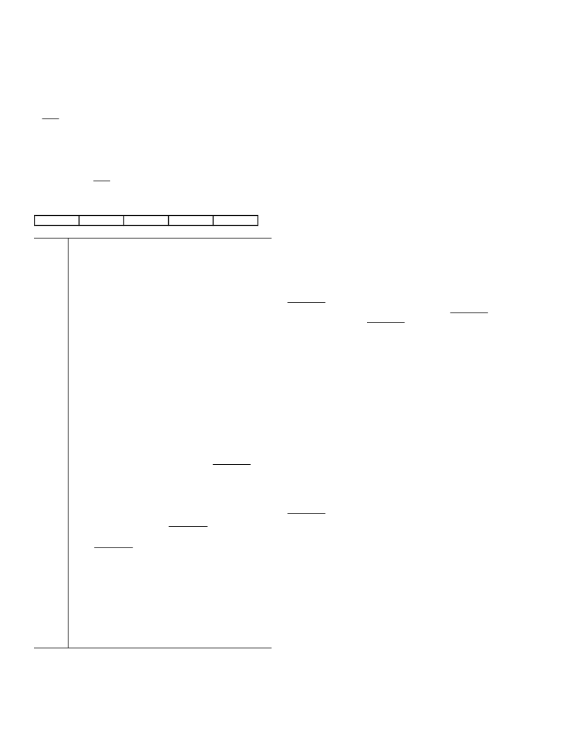
CONT ROL RE GIST E R
T he Control Register for the AD7890 contains 5 bits of infor-
mation as described below. Six serial clock pulses must be pro-
vided to the part in order to write data to the Control Register
(seven if the write is required to put the part in Standby Mode).
If
TFS
returns high before six serial clock cycles then no data
transfer takes place to the Control Register and the write cycle
will have to be restarted to write the data to the Control Regis-
ter. If, however, the CONV bit of the register (see below) is set
to a Logic 1, then a conversion will be initiated whenever a
Control Register write takes place regardless of how many serial
clock cycles the
TFS
remains low for. T he default (power-on)
condition of all bits in the Control Register is 0.
MSB
A2
A1
A0
C ONV
ST BY
A2
Address Input. T his input is the most significant
address input for multiplexer channel selection.
A1
Address Input. T his is the 2nd most significant
address input for multiplexer channel selection.
A0
Address Input. Least significant address input for
multiplexer channel selection. When the address is
written to the control register, an internal pulse is
initiated, the pulse width of which is determined by
the value of capacitance on the C
EX T
pin. When this
pulse is active, it ensures the conversion process
cannot be activated. T his allows for the multiplexer
settling time and track/hold acquisition time before
the track/hold goes into hold and conversion is
initiated. In applications where there is an anti-
aliasing filter between MUX OUT and SHA IN, the
filter settling time can be taken into account before
the input at SHA IN is sampled. When the internal
pulse times out, the track/hold goes into hold and
conversion is initiated.
CONV
Conversion Start. Writing a 1 to this bit initiates a
conversion in a similar manner to the
CONVST
input. Continuous conversion starts do not take place
when there is a 1 in this location. T he internal pulse
and the conversion process are initiated after the
sixth serial clock cycle of the write operation if a 1 is
written to this bit. With a 1 in this bit, the hardware
conversion start i.e., the
CONVST
input, is
disabled. Writing a 0 to this bit enables the hard-
ware
CONVST
input.
ST BY
Standby Mode Input. Writing a 1 to this bit places
the device in its standby or power-down mode.
Writing a 0 to this bit places the device in its normal
operating mode. T he part does not enter its standby
mode until the seventh falling edge of SCLK in a
write operation. T herefore, the part requires seven
serial clock pulses in its serial write operation if it is
required to put the part into standby.
CONVE RT E R DE T AILS
T he AD7890 is an eight-channel, 12-bit, single supply, serial
data acquisition system. It provides the user with signal scaling,
multiplexer, track/hold, reference, A/D converter and versatile
serial logic functions on a single chip. T he signal scaling allows
the part to handle
±
10 V input signals (AD7890-10) and 0 V to
+4.096 V input signals (AD7890-4) while operating from a
single +5 V supply. T he AD7890-2 contains no signal scaling
and accepts an analog input range of 0 V to +2.5 V. T he part
operates from a +2.5 V reference which can be provided from
the part’s own internal reference or from an external reference
source.
Unlike other single chip data acquisition solutions, the AD7890
provides the user with separate access to the multiplexer and the
A/D converter. T his means that the flexibility of separate multi-
plexer and ADC solutions is not sacrificed with the one-chip
solution. With access to the multiplexer output, the user can
implement external signal conditioning between the multiplexer
and the track/hold. It means that one antialiasing filter can be
used on the output of the multiplexer to provide the antialiasing
function for all eight channels.
Conversion is initiated on the AD7890 either by pulsing the
CONVST
input or by writing a Logic 1 to the CONV bit of the
Control Register. When using the hardware
CONVST
input, on
the rising edge of the
CONVST
signal, the on-chip track/hold
goes from track to hold mode and the conversion sequence is
started provided the internal pulse has timed out. T his internal
pulse (which appears at the C
EX T
pin) is initiated whenever the
multiplexer address is loaded to the AD7890 Control Register.
T his pulse goes from high to low when a serial write to the part
is initiated. It starts to discharge on the sixth falling clock edge
of SCLK in a serial write operation to the part. T he track/hold
cannot go into hold and conversion cannot be initiated until the
C
EX T
pin has crossed its trigger point of 2.5 V. T he discharge
time of the voltage on C
EX T
depends upon the value of capacitor
connected to the C
EX T
pin (see C
EX T
Functioning section). T he
fact that the pulse is initiated every time a write to the control
register takes place means that the software conversion start and
track/hold signal is always delayed by the internal pulse.
T he conversion clock for the part is generated from the clock
signal applied to the CLK IN pin of the part. Conversion time
for the AD7890 is 5.9
μ
s from the rising edge of the hardware
CONVST
signal and the track/hold acquisition time is 2
μ
s. T o
obtain optimum performance from the part, the data read opera-
tion or Control Register write operation should not occur during
the conversion or during 500 ns prior to the next conversion.
T his allows the part to operate at throughput rates up to
117 kHz in the external clocking mode and achieve data sheet
specifications. T he part can operate at slightly higher through-
put rates (up to 127 kHz), again in external clocking mode with
degraded performance (see T iming and Control section). T he
throughput rate for self-clocking mode is limited by the serial
clock rate to 78 kHz.
All unused inputs should be connected to a voltage within the
nominal analog input range to avoid noise pickup. On the
AD7890-10, if any one of the input channels which are not be-
ing converted goes more negative than –12 V, it can interfere
with the conversion on the selected channel.
相關PDF資料 |
PDF描述 |
|---|---|
| AD7890BR-10 | LC2MOS 8-Channel, 12-Bit Serial, Data Acquisition System |
| AD7890BR-2 | LC2MOS 8-Channel, 12-Bit Serial, Data Acquisition System |
| AD7890BR-4 | LC2MOS 8-Channel, 12-Bit Serial, Data Acquisition System |
| AD7890AR-10 | Side Entry Connector Hood; Enclosure Material:Aluminum Alloy; For Use With:C146 Rectangular Circular Connectors; Connecting Termination:Screw; Gender:Male; No. of Contacts:48; Operating Voltage:400V; Series:C-146 RoHS Compliant: Yes |
| AD7890AR-2 | Circular Connector Cable Assembly; Connector Type A:Circular Receptacle; Connector Type B:Stripped End Leads; Cable Length:10ft; Features:500 Mating Cycles, PVC Jacket, IP67 Rating, E63093 Rated Connector; No. of Contacts:6 RoHS Compliant: Yes |
相關代理商/技術參數 |
參數描述 |
|---|---|
| AD7890BNZ-10 | 功能描述:IC DAS 12BIT 8CH 24-DIP RoHS:是 類別:集成電路 (IC) >> 數據采集 - ADCs/DAC - 專用型 系列:- 產品培訓模塊:Lead (SnPb) Finish for COTS Obsolescence Mitigation Program 標準包裝:50 系列:- 類型:數據采集系統(DAS) 分辨率(位):16 b 采樣率(每秒):21.94k 數據接口:MICROWIRE?,QSPI?,串行,SPI? 電壓電源:模擬和數字 電源電壓:1.8 V ~ 3.6 V 工作溫度:-40°C ~ 85°C 安裝類型:表面貼裝 封裝/外殼:40-WFQFN 裸露焊盤 供應商設備封裝:40-TQFN-EP(6x6) 包裝:托盤 |
| AD7890BNZ-2 | 功能描述:IC DAS 12BIT 8CH 24-DIP RoHS:是 類別:集成電路 (IC) >> 數據采集 - ADCs/DAC - 專用型 系列:- 產品培訓模塊:Lead (SnPb) Finish for COTS Obsolescence Mitigation Program 標準包裝:50 系列:- 類型:數據采集系統(DAS) 分辨率(位):16 b 采樣率(每秒):21.94k 數據接口:MICROWIRE?,QSPI?,串行,SPI? 電壓電源:模擬和數字 電源電壓:1.8 V ~ 3.6 V 工作溫度:-40°C ~ 85°C 安裝類型:表面貼裝 封裝/外殼:40-WFQFN 裸露焊盤 供應商設備封裝:40-TQFN-EP(6x6) 包裝:托盤 |
| AD7890BNZ-4 | 功能描述:IC DAS 12BIT 8CH 24-DIP RoHS:是 類別:集成電路 (IC) >> 數據采集 - ADCs/DAC - 專用型 系列:- 產品培訓模塊:Lead (SnPb) Finish for COTS Obsolescence Mitigation Program 標準包裝:50 系列:- 類型:數據采集系統(DAS) 分辨率(位):16 b 采樣率(每秒):21.94k 數據接口:MICROWIRE?,QSPI?,串行,SPI? 電壓電源:模擬和數字 電源電壓:1.8 V ~ 3.6 V 工作溫度:-40°C ~ 85°C 安裝類型:表面貼裝 封裝/外殼:40-WFQFN 裸露焊盤 供應商設備封裝:40-TQFN-EP(6x6) 包裝:托盤 |
| AD7890BR-10 | 功能描述:IC DAS 12BIT 8CH 24-SOIC RoHS:否 類別:集成電路 (IC) >> 數據采集 - ADCs/DAC - 專用型 系列:- 產品培訓模塊:Lead (SnPb) Finish for COTS Obsolescence Mitigation Program 標準包裝:50 系列:- 類型:數據采集系統(DAS) 分辨率(位):16 b 采樣率(每秒):21.94k 數據接口:MICROWIRE?,QSPI?,串行,SPI? 電壓電源:模擬和數字 電源電壓:1.8 V ~ 3.6 V 工作溫度:-40°C ~ 85°C 安裝類型:表面貼裝 封裝/外殼:40-WFQFN 裸露焊盤 供應商設備封裝:40-TQFN-EP(6x6) 包裝:托盤 |
| AD7890BR-10REEL | 功能描述:IC DAS 12BIT 8CH 24-SOIC RoHS:否 類別:集成電路 (IC) >> 數據采集 - ADCs/DAC - 專用型 系列:- 產品培訓模塊:Lead (SnPb) Finish for COTS Obsolescence Mitigation Program 標準包裝:50 系列:- 類型:數據采集系統(DAS) 分辨率(位):16 b 采樣率(每秒):21.94k 數據接口:MICROWIRE?,QSPI?,串行,SPI? 電壓電源:模擬和數字 電源電壓:1.8 V ~ 3.6 V 工作溫度:-40°C ~ 85°C 安裝類型:表面貼裝 封裝/外殼:40-WFQFN 裸露焊盤 供應商設備封裝:40-TQFN-EP(6x6) 包裝:托盤 |
發布緊急采購,3分鐘左右您將得到回復。